Chinese semiconductor thread II

tokenanalyst

Brigadier
Registered Member

Nanya New Materials plans to invest 1.2 billion yuan in the construction of a high-end electronic circuit base material base project​

Nanya New Materials announced on the evening of March 26 that based on the needs of the overall strategic layout and business development, in order to speed up production capacity planning and industrial layout, it plans to invest in the construction of
According to the Big Semiconductor Industry Network, Nanya New Materials announced on the evening of March 26 that based on the needs of the overall strategic layout and business development, in order to speed up production capacity planning and industrial layout, it plans to invest in the construction of a high-end electronic circuit substrate base construction project.
According to the announcement, the project has a total investment of 1.2 billion yuan and will be implemented by Jiangsu Nanya, a wholly-owned subsidiary. It plans to purchase land to build a new production base in Haimen Economic and Technological Development Zone, Jiangsu Province. This project is divided into a high-end IC carrier board material industrialization construction project and a high-end copper clad laminate industrialization construction project. The construction period is expected to be 4 years.
Nanya New Materials said that by building a high-end electronic circuit substrate base, the project will support the company's future industrialization needs for high-frequency, high-speed and IC packaging materials and other high-end electronic substrates, thereby meeting the demand for expansion of high-end electronic circuit substrate production lines. , is conducive to promoting the development of electronic material technology, and is of great significance to the implementation of the national development strategic plan. In addition, the project will provide supporting conditions for the mass production of existing research and development results, new processes and new products, which will help enhance the company's core competitiveness and consolidate the company's dominant position in the high-end materials industry.

Please, Log in or Register to view URLs content!
 

tphuang

Lieutenant General
Staff member
Super Moderator
VIP Professional
Registered Member
Yandong Micro, best known for using SMEE DUV lithography in its 65nm process has reported its 2023 results

Please, Log in or Register to view URLs content!

revenue down 2.2% YoY

It's 12-inch line started production in July of last year with 7.5B RMB investment. Planned production of 40k wpm for high density power chips, display IC, PMIC and optoelectronics chips. It has also started production of SiC-SBD products in 6-inch line
 

sunnymaxi

Captain
Registered Member

Zhijing Micro releases extremely high-precision 24MHz rail-to-rail input and output CMOS operational amplifier ZJA3216​


Shanghai Zhijing Microelectronics Co., Ltd. (hereinafter referred to as "Zhijing Micro"), a high-end analog chip solution provider headquartered in Zhangjiang, grandly launches the new 5 V high-precision rail-to-rail input and output CMOS operational amplifier ZJA3 216 . It is the first precision low-voltage operational amplifier successfully developed by Zhijingwei after the 36 V general-purpose precision amplifier ZJA3000 , JFET amplifier ZJA3512 , instrumentation amplifier ZJA3600 , and differential amplifier ZJA3676 series. It not only supplements and improves Zhijingwei ’s amplifier product line, but also It fills the gap in the field of high-precision general-purpose continuous amplifiers in China. The table in Figure 1 provides a comparison of the main technical indicators of ZJA 3216 and international competing products.

Please, Log in or Register to view URLs content!
 

Jamie28

New Member
Registered Member
Yandong Micro, best known for using SMEE DUV lithography in its 65nm process has reported its 2023 results

Please, Log in or Register to view URLs content!

revenue down 2.2% YoY

It's 12-inch line started production in July of last year with 7.5B RMB investment. Planned production of 40k wpm for high density power chips, display IC, PMIC and optoelectronics chips. It has also started production of SiC-SBD products in 6-inch line

Are they using the SSA800?
 

Schmoe

New Member
Registered Member
"Yandong Micro, best known for using SMEE DUV lithography in its 65nm process has reported its 2023 results"

Is that the first known use of an SMEE DUV machine in a production line? If so, I wonder if it is possible to make any assumptions about production or yield rates.
 
Last edited:

tokenanalyst

Brigadier
Registered Member

Two SiC R&D centers were officially launched​


Recently, two SiC-related R&D centers jointly built by Tianyue Semiconductor, a subsidiary of Tianyue Advanced Semiconductor, and Shanghai Ruineng Weilan Semiconductor, a subsidiary of Ruineng Semiconductor, were officially launched.
"Yangtze River Delta National Technology Innovation Center-Tianyue Semiconductor Joint Innovation Center" was unveiled On March 26, the "2024 Lingang Science and Technology Innovation Conference" was held at Shanghai Lingang Center. The "Yangtze River Delta National Technology Innovation Center-Tianyue Semiconductor Joint Innovation Center" held an unveiling ceremony at this conference. The joint innovation center will realize the transformation from science to technology through the deep integration of industry, academia and research, and promote the research of key core technologies in the field of SiC semiconductors.​

Please, Log in or Register to view URLs content!
 

tokenanalyst

Brigadier
Registered Member

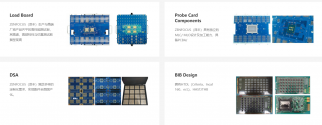
Zefeng: The entire series of probe cards is “under control”, and breakthrough progress has been made to build the “localization” of all components​


Zefeng made a major appearance at the two major exhibitions with three major categories of products and two major categories of solutions, demonstrating its high-level domestic independent material research and development capabilities, mature process capabilities and excellent factory manufacturing capabilities. Cutting-edge products and solutions coupled with hard-core technology and excellent design have attracted customer groups from all over the country to stop for consultation, and the store was once crowded.

Among them, the three major categories of products on display include MEMS probe cards, ATE test boards and ceramic substrates. In terms of probe cards, Zefeng has successfully independently developed and grandly launched the interstellar series product matrix based on years of technology accumulation: covering from CPC to VPC to high-end 3D MEMS probe cards. This time On display were the Large Magellanic Cloud probe card (LMC, adapted for high-end memory chip testing) and the Mars series probe card (Mars, adapted for pan-storage, MCU and other functional chip testing). Once they were unveiled, they attracted strong attention from many attendees.

Zefeng exhibited a complete FT/CP high-speed ATE test solution developed based on the MultiLane platform. The μBump bonding technology it adopted emerged as a smaller interface connection technology, which can fully meet the requirements of advanced packaging for connecting chips and The demand for substrate bridging technology helps partners improve ATE test efficiency and reduce test costs.

Advanced ceramic products are also Zefeng's star products at this exhibition, including 12-inch LTCC ceramic substrates, ceramic tube shells, T/R components, etc., which achieve high-density multi-layer design through production processes, which can fully meet the needs of advanced packaging The demand for high linear density substrates has not only attracted research institutes to come for exchanges and media visits, but also an endless stream of inquiries from visitors.

1711590097078.png
1711590144315.png

Please, Log in or Register to view URLs content!
 
Top