Chinese semiconductor thread II

tokenanalyst

Brigadier
Registered Member

Hefei New Station starts construction of new semiconductor project to build photoresist core main material mass production base​

March 26, the groundbreaking ceremony of Weimai Core Materials (Hefei) Semiconductor Co., Ltd.'s annual output of 100 tons of semiconductor high-end photolithography materials project was held in Hefei Xinzhan High-tech Zone. After the project is put into production, localized supply of key photoresist materials will be achieved, which is of great significance to the stable development of the local integrated circuit industry.

Weimai Core Material (Hefei) Semiconductor Co., Ltd. is a wholly-owned subsidiary of Suzhou Weimai. It is located at the intersection of Yingzhou Road and Longzihu Road in Xinzhan High-tech Zone. It covers an area of 50 acres and has a total investment of 300 million yuan. It aims to Build the largest high-end semiconductor DUV-level (ArF/KrF) photoresist core main material mass production base in China. Products include photoacid generator PAG, BARC layer resin Resin, photoinitiator PI, etc. It also provides intermediates and core monomer materials for each final product. It is planned to build an annual production capacity of 100 tons and will be completed and put into use by the end of the year. .

It is understood that Weimax Core Materials has always focused on the R&D and production of high-end semiconductor DUV-level (ArF/KrF) photoresist core main materials. With core technologies such as PPB-level metal impurity control and multi-step synthesis customized development, it has Successfully imported into many leading domestic photoresist companies such as Fuyang Xinyihua, Nanda Optoelectronics, Suzhou Ruihong, Beijing Kehua Micro, Xuzhou Bokang, Wuhan Dinglong, etc., becoming the leading supplier of domestic PAG for Chinese photoresist companies.

Please, Log in or Register to view URLs content!
 

tphuang

Lieutenant General
Staff member
Super Moderator
VIP Professional
Registered Member
Please, Log in or Register to view URLs content!

SMEC FY report and you can see the trajectory of their revenue here. Huge growth, but they are probably still losing money due to high depreciation costs.

47% of chip comes from auto grade chips and another 29% comes from industrial control. Remaining are MEMS and other high end consumer elctronics
 

tokenanalyst

Brigadier
Registered Member

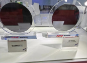
CETC epitaxial wafers at Semicon China 2024​


1711495261328.png


 In the field of integrated circuit equipment, key core equipment such as ion implanters, wet cleaning, vertical furnaces, and thinning and dicing were displayed. Among them, medium-beam, large-beam, high-energy machines and special application ion implanters have been domestically produced in the entire series, reaching full coverage of the 28nm process; cleaning equipment has a variety of wet methods such as semiconductor cleaning, wet etching, electroplating ECD and stripping. process; vertical furnaces form a series of products such as oxidation, diffusion, annealing, alloying, and low-pressure chemical vapor deposition; thinning, dicing and other packaging equipment are continuously supplied to well-known domestic leading companies in large quantities.

 In the field of compound semiconductor equipment, it demonstrated the R&D and industrialization capabilities of more than 40 types of core equipment covering the entire process section including crystal growth, material processing, epitaxial growth, high-temperature injection, packaging and assembly, inspection and testing, demonstrating the country's only complete set of compound semiconductor equipment to solve The capability level of the solution capability provider.

In the field of microsystems, a series of key core equipment such as system layout PVD, ECD, high-precision flip-chip welding, wafer temporary bonding and debonding, and wafer permanent bonding plasma cleaning were demonstrated, aiming at "core breakthroughs, partial complete sets, and systems "Integration" direction, and strive to create practical results of system integration services for the entire production line of microsystem manufacturing.

  In the field of semiconductor materials, a variety of products such as silicon-based gallium nitride epitaxy, silicon carbide single crystal substrate, silicon carbide epitaxy, and silicon epitaxy were displayed. The manufacturing level of silicon carbide single crystal substrate, silicon carbide epitaxy, and silicon epitaxy is domestically leading.

Please, Log in or Register to view URLs content!
 

measuredingabens

Junior Member
Registered Member
Please, Log in or Register to view URLs content!

Please, Log in or Register to view URLs content!

Pixelated non-volatile programmable photonic integrated circuits proposed by researchers in China

Researchers from Huazhong University of Science and Technology proposed a pixelated programmable photonic integrated circuit (PICs) with record-high 20-level intermediate states of phase change materials (PCMs).

The work,
Please, Log in or Register to view URLs content!
in the International Journal of Extreme Manufacturing, could pave the way for the applications of laser-induced PCMs in neuromorphic photonics, optical computing, and reconfigurable metasurfaces.

Prof. Jinlong Zhu, corresponding author at the School of Mechanical Science and Engineering of HUST explains, "The research on programmable PCMs-based PICs and metasurfaces primarily utilized thermal annealing and electrothermal switching. In contrast, multi-level PCMs with free-space laser switching offer significantly enhanced flexibility in phase modulation."

Programmable PICs have emerged as powerful platforms in a variety of fields, such as optical communications, sensors, and photonic neural networks. Due to the large refractive index contrast (∆n >1 ) between the amorphous and crystalline states of chalcogenide PCMs, researchers have investigated PCMs in nanophotonic platforms to perform programmable optical functions.

While there has been significant research development on low-loss PCMs in the amorphous and crystalline states, the study of the multi-level intermediate states at the micron scale is still in its infancy. The research on programmable PCMs-based PICs and metasurfaces primarily utilized thermal annealing and electrothermal switching.


As a result, programmable PICs and metasurfaces with ultra-high flexibility in phase modulation using multi-level PCMs with free-space laser switching were rarely reported.

The researchers investigated the laser-writing multi-level intermediate states of a single Sb2S3 element at the microscale. By optimizing the power and quantity of laser pulses, 20-level intermediate states of single Sb2S3 pixels were realized in the range of 120 ~ 320 pulses. The diameter of the phase-transition pixels is about 1.2 μm, which is caused by the focused laser.

By utilizing multi-level intermediate states achieved by micron-scale laser writing system, the researchers simulated an Sb2S3-based phase shifter in a programmable Mach-Zehnder interferometer and demonstrated that it could achieve 30-level phase shift accuracy of π at 785 nm wavelength. In this way, the availability of very large-scale pixelated non-volatile programmable PICs has been demonstrated by simulation.

The Sb2S3-matrix-based programmable photonic integrated circuits could have a positive impact on general-purpose programmable photonic circuits and photonic neural networks. Moreover, the applications of
Please, Log in or Register to view URLs content!
-induced programmable devices open up for neuromorphic photonics, optical computing, and reconfigurable metasurfaces.

The researchers are continuing the work, applying pixelated programmable phase change materials to programmable photonic integrated circuits and metasurfaces.
 

tokenanalyst

Brigadier
Registered Member

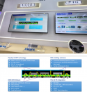
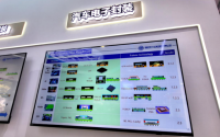
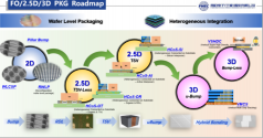
Yongsilicon Electronics automotive wafer level packaging​


Yongsilicon Electronics is actively deploying chiplet-based advanced Fan-in/Fan-out, WLCSP, 2.5D/3D and other wafer-level packaging technologies, and has successfully developed multi-chip fan-out heterogeneous Integrated packaging (Multi-Chip Fan-Out) technology; completed the development and mass production of large FC-BGA technology for computing, servers and other fields, and is expected to seize the development opportunities of the advanced packaging industry.

1711552492645.png1711552694972.png
1711552734696.png

Please, Log in or Register to view URLs content!
 
Top