Chinese semiconductor thread II

tokenanalyst

Lieutenant General
Registered Member
You don't need EUV for 32nm lithography?
Back then, the overlay issue was not solved, so keep the Critical Dimension high, transistors planar and use single patterning to ensure good yields and decent throughputs. Now looks like is solved, looks like the are going multi-patterning 3D transistor.
The same way that the Russians plan to do with their lithography machines large feature sizes and single patterning 45nm planar despite the resolution being 6.5nm to make placement errors redundant.
 

sunnymaxi

Colonel
Registered Member
China has developed many prototypes over the years. In 2016, they developed a prototype of a 90nm lithography machine. In 2023 they developed a prototype of a 28nm lithography machine. Now they have supposedly developed a prototype of an EUV lithography machine. The problem is that we have never heard proof that any of these prototypes ever made it to the mass production for commercial use stage. The only machines in use for mass production are ASML, and to a lesser extent, Nikon and Canon. At this point, I'd be more impressed with a confirmed report of any Chinese front end lithography machine of any node size in use for mass production on a commercial line, than another prototype of even the most advanced capability.
domestic immersion scanner has applied on few lines and they continue to improve machine till now.. Lithography is just one piece of the entire puzzle. you also need photomask , photoresist , inspection tool for Litho.

the issue is, nobody cares about 65nm/44nm/28nm chips. i don't think so any entity will purchase mature chip and tear it up then examine whether it is made with domestic scanner or foreign machine. everybody runs toward 7nm.

that 90nm machine has discarded and they developed new 65nm machine in 2022.

28nm immersion scanner testing and evaluation taking so much time. which is normal for such a complex machine.

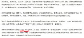
Yandong fab is in Beijing, they have been using 100 percent domestic tools.. up until recently they were using dry scanner but last week they announced 28nm line. all set to mass produce 28m chips with immersion machine..

Yandong domestic 28nm line Q2,2026.jpg
 

chlosy

Junior Member
Registered Member
"The Netherlands exported US$6.8 billion worth of lithography machines to China in the first 10 months of this year. That made them the EU’s top-earning export to China, the same position they occupied last year.

Please, Log in or Register to view URLs content!
, the Dutch company that is the world’s top supplier of advanced chipmaking equipment, ships products to China that are eight generations, or more than 10 years, behind what it sells in the West, CEO Christophe Fouquet told Bloomberg TV in a recent interview."

From SCMP

Is this accurate? USD6.8 billion worth of older generation stuff??? What percentage of the Chinese market is this?
 

tokenanalyst

Lieutenant General
Registered Member
China has developed many prototypes over the years. In 2016, they developed a prototype of a 90nm lithography machine. In 2023 they developed a prototype of a 28nm lithography machine. Now they have supposedly developed a prototype of an EUV lithography machine. The problem is that we have never heard proof that any of these prototypes ever made it to the mass production for commercial use stage. The only machines in use for mass production are ASML, and to a lesser extent, Nikon and Canon. At this point, I'd be more impressed with a confirmed report of any Chinese front end lithography machine of any node size in use for mass production on a commercial line, than another prototype of even the most advanced capability.
But that is the problem, stooges ignoring past developments is peek stooge arrogance, first of all they didn´t know how advanced these prototypes where before saying "China can´t even make EUV mirrors", how many 300mm WPH the devices could pattern back then, even 10 WPH is a big development. I saw the tray of the prototype of 2016 and have space for at least 20 300mm wafers. Second, China EUV and lithography development in general never stopped, if you go to the research and patent literature you could find that the development never stopped. If you remove the arrogant chip from the head, before banning almost 10 generations of lithography machines, you can find that China lithography machines development NEVER STOPPED. The biggest difference from the last 5 years to back them is that now you have the biggest, best organize semiconductor companies in China and the world behind this development, Huawei, SMIC, YMTC and many others. While in the past was only the government and SMEE.
 

Phead128

Major
Staff member
Moderator - World Affairs
China has developed many prototypes over the years. In 2016, they developed a prototype of a 90nm lithography machine. In 2023 they developed a prototype of a 28nm lithography machine. Now they have supposedly developed a prototype of an EUV lithography machine. The problem is that we have never heard proof that any of these prototypes ever made it to the mass production for commercial use stage. The only machines in use for mass production are ASML, and to a lesser extent, Nikon and Canon. At this point, I'd be more impressed with a confirmed report of any Chinese front end lithography machine of any node size in use for mass production on a commercial line, than another prototype of even the most advanced capability.
Looks like you at stage 2 of tech denial/copium curve.
  1. It's not a "real" EUV, just a SeeSeePee propaganda.
  2. Okay it's an actual prototype, but just a lab test unit for research use.
  3. Okay, it's commercial grade, but low-yields, costly, economic suicide. At what cost?
  4. Okay, decent yields, but it was espionage, stolen, reverse engineered.
  5. Okay, even if they figured out a lot themselves, but limited scalability and capacity. Unclear performance parameters.
  6. Okay, decent capacity, but "only" Chinese customers, no Western market or export appeal.
  7. Okay, EUV exports, but not high-NA!
  8. Okay, high-NA, but let me sell you ASML EUV to get you addicted to Western tech stack.
  9. Okay, you have legit high-NA EUV, but that's dangerous overcapacity and national security concern, must ban!
  10. Overall, EUV is junk tier technology that even primitives can do, boring. Legacy stone age tools. Try jet engine tech, does WS-10 do better than 400 hrs MTBF?
Exclusive: How China built its ‘Manhattan Project’ to rival the West in AI chips
Please, Log in or Register to view URLs content!
Reuters article riddled with disinformation and flaws that tries to undersell the vast monumental challenge of "
Please, Log in or Register to view URLs content!
" as NYT calls it, which is replicating an independent supply chain for semiconductors and developing EUV.
The availability of parts from older ASML machines on secondary markets has allowed China to build a domestic prototype, with the government setting a goal of producing working chips on the prototype by 2028, according to the two people. (
Please, Log in or Register to view URLs content!
)................Export-restricted components from Japan’s Nikon and Canon are being used for the prototype, one of the people and an additional source said. (
Please, Log in or Register to view URLs content!
)
How did they conclude "second hand DUV parts" from Nikon and Canon can make assemble EUV? DUV is fundamentally different from EUV...and it is not interchangeable Lego pieces... This gives off "Russia is recycling washing machine chips" vibes.

It was built by a team of former engineers from Dutch semiconductor giant ASML who reverse-engineered the company's extreme ultraviolet lithography machines or EUVs, according to two people with knowledge of the project. (
Please, Log in or Register to view URLs content!
)
...................
No EUV system has ever been sold to a customer in China, ASML told Reuters. (
Please, Log in or Register to view URLs content!
)
How did they conclude 'reverse engineering' without ASML shipping an actual EUV unit on hand to disassemble, analyze, and inspect? You can't really call it 'reverse engineering' without an EUV sample unit on-hand. Rather, the more appropriate term is 'indigenous innovation' or 'independent re-implementation', let's not devalue this as simply copy-paste, it's a monumental task to re-implement this technology independent without a working unit in front of you.
The team includes recently retired, Chinese-born former ASML engineers and scientists—prime recruitment targets because they possess sensitive technical knowledge but face fewer professional constraints after leaving the company, the people said. (
Please, Log in or Register to view URLs content!
).............. The company said it safeguards EUV knowledge by ensuring only select employees can access the information even inside the company. (
Please, Log in or Register to view URLs content!
)
I am sure it's helpful to have former ASML engineers to contribute knowledge, but even ASML admits only a select few engineers have access to the core technology or know-how of the entire system itself. It is deeply misleading to suggest that hiring a limited number of former ASML employees would be sufficient to recreate an EUV system from scratch. ASML engineers are typically specialists, each focused on a narrow component or process within a highly complex, multi stage workflow. Even if you take it to the extreme by recruiting the entirety of ASML’s engineering staff would still be insufficient without the underlying materials science, supplier ecosystems, and manufacturing capabilities required to actually implement the tech, rather than simply understand its theoretical steps. You have to master the underlying industrial processes to implement it in practice, not just hire the fragmented bits of knowledge behind it for pennies on the dollar.

A team of around 100 recent university graduates is focused on reverse-engineering components from both EUV and DUV lithography machines, according to the people. (
Please, Log in or Register to view URLs content!
)
First off, this is a "Manhattan level project", yet it relies on a team of 100 recent university graduates to allegedly hand-disassemble and reassemble? REALLY? Has China run out of professional seasoned engineers like "Russia has run out of missiles"? This also gives me "China throws cheap bodies in human waves at problem" vibes. Really, only 100 recent university graduates? Try tens of thousands of seasoned engineers and professional scientist with decades of scientific experience, not a bunch of noobs led by a few Western-trained ASML specialists.
 

Clark Gap

Junior Member
Registered Member
From following the forums, I haven't seen any rumors of a working EUV chip from China yet. I'd love to be wrong, but we should be cautiously optimistic to avoid false expectations. We'll probably hear more about it by 2026-2027; that's my hope, anyway.
Domestic EUV lithography machines will not first be applied to logic chips, but to memory chips. Memory chips also require EUV technology, though with less demanding specifications. So just keep an eye on CXMT’s product lineup.
 

Maikeru

Major
Registered Member
"The Netherlands exported US$6.8 billion worth of lithography machines to China in the first 10 months of this year. That made them the EU’s top-earning export to China, the same position they occupied last year.

Please, Log in or Register to view URLs content!
, the Dutch company that is the world’s top supplier of advanced chipmaking equipment, ships products to China that are eight generations, or more than 10 years, behind what it sells in the West, CEO Christophe Fouquet told Bloomberg TV in a recent interview."

From SCMP

Is this accurate? USD6.8 billion worth of older generation stuff??? What percentage of the Chinese market is this?
Don't know about that but ASML is down >8% since this news broke.
 

supersnoop

Colonel
Registered Member
First off, this is a "Manhattan level project", yet it relies on a team of 100 recent university graduates to allegedly hand-disassemble and reassemble? REALLY? Has China run out of professional seasoned engineers like "Russia has run out of missiles"? This also gives me "China throws cheap bodies in human waves at problem" vibes. Really, only 100 recent university graduates? Try tens of thousands of seasoned engineers and professional scientist with decades of scientific experience, not a bunch of noobs led by a few Western-trained ASML specialists.
I think this was one of the most egregious implications in the article. Like a lithography machine is some kind of 50’s car where some Bubba mechanic can take apart the carburetor and put it back together again in his garage… Oh here’s a bonus by the way! As if these people went to years of school and have no understanding of underlying fundamentals to develop something. I guess you still need to push that West/ASML is best narrative some how.
 
Top