Chinese semiconductor thread II

tokenanalyst

Lieutenant General
Registered Member

AMEC's acquisition of Hangzhou Zhonggui's equity is finalized.​


Advanced Micro-Fabrication Equipment (Shanghai) Co., Ltd. (AMEC) has finalized its strategic acquisition of a controlling 64.69% stake in Hangzhou Zhonggui, addressing a critical gap in the domestic wet process semiconductor sector. Valued at approximately RMB 2.436 billion for the full equity, this deal marks AMEC's transition from a provider of single dry-process capabilities to one of the few national platforms covering four core front-end technologies: etching, thin film deposition, metrology, and now wet processes via CMP equipment. To ensure the transaction's stability, AMEC simultaneously launched a supporting fundraising scheme aimed at raising up to RMB 1.5 billion through share issuance with specific targets; however, this financing step is separate from the core asset acquisition, guaranteeing that the deal proceeds regardless of the final fund-raising outcome while providing necessary capital for construction and integration.

The strategic significance of this move lies in its ability to decouple AMEC's high-end CMP technology, which had previously relied heavily on overseas manufacturers, and integrate it with existing domestic dry-process solutions. By acquiring Hangzhou Zhonggui a leader in mass-producing 12-inch high-end CMP equipment AMEC drastically shortens the verification cycles for wafer manufacturing firms and enhances supply chain self-reliance across advanced logic, memory, and packaging sectors. Analysts view this as a pivotal leapfrog upgrade that not only strengthens AMEC's market competitiveness but also injects robust momentum into China's broader semiconductor industry chain, solidifying its position as a leader capable of delivering comprehensive, fully domestic equipment solutions.

Please, Log in or Register to view URLs content!
 

tokenanalyst

Lieutenant General
Registered Member

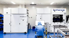
Ingenics has established its headquarters in Optics Valley, where it is developing domestically produced "light-generating mother machines".​


On July 7, with the signing of the agreement by Ingenics Technology Co., Ltd. (hereinafter referred to as "Ingenics") to settle in Wuhan Future Science and Technology City, a key piece of the puzzle of MOCVD equipment will be completed.
English-Chinese R&D Scenarios

Founded in 2024, Ingenic focuses on the research and development and production of MOCVD equipment. MOCVD is a key epitaxial device for compound semiconductor optoelectronic devices. Through chemical vapor deposition, it grows a single-crystal thin film on a substrate that determines the photoelectric performance of the chip. Without this "foundation", the chip cannot be "grown". Therefore, MOCVD is also known as the "photonics mother machine".

1783524568107.png1783524610246.png

InHanSi is one of the few domestic companies that can simultaneously cover multiple semiconductor material systems such as gallium nitride, gallium carbide, gallium arsenide, and indium phosphide, corresponding to mainstream application scenarios such as mobile phone fast charging chips, 5G base station power devices, and new energy vehicle power modules.

The Chairman of Ingenic Semiconductor, stated that Optics Valley boasts a highly efficient and supportive business environment with a favorable industrial foundation, allowing semiconductor companies to complete all stages from R&D to production within a few kilometers. After settling in, the company will collaborate with the Jiufengshan Laboratory and upstream and downstream enterprises within the area to accelerate the R&D iteration and production delivery of domestically produced MOCVD equipment.

The company has already started equipment debugging in Optics Valley and will move into the High-Tech Laser Industry Base to build a production base with an area of over 2,000 square meters, so as to achieve batch shipment of multiple models of MOCVD equipment.

Optics Valley has attracted more than 300 integrated circuit companies. Among them, Jiufengshan Laboratory, as the main unit of the compound semiconductor chain, has attracted more than 50 upstream and downstream companies to settle in Optics Valley since its establishment in 2021, forming a complete industrial chain covering compound semiconductor materials, devices and packaging and testing.​

Please, Log in or Register to view URLs content!
 

tokenanalyst

Lieutenant General
Registered Member

From SPAD chips to AI optical interconnects: The system-level leap behind Lingming Photonics' "dual-track positioning"​


Hangzhou-based Lingming Photonics has successfully attracted significant capital with a strategic 300 million RMB investment from A-share listed company Zhiyang Innovation. This move is part of a broader ecosystem involving provincial state-owned assets and major industrial players like Xiaomi, OPPO, and Lenovo. The core logic behind this backing is Lingming's profound transformation from a single-chip manufacturer into an "underlying technology platform" for the AI era. By shifting its focus to provide integrated hardware-software perception solutions, the company aims to navigate industry cycles while opening up long-term growth spaces in both consumer robotics and industrial automation sectors.

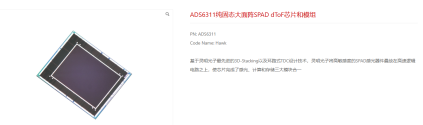
Lingming's business strategy is anchored by two divergent but complementary revenue streams designed to hedge against market volatility. On one hand, its automotive laser radar chip division has established itself as a domestic leader, with shipments reaching record levels in 2025 driven by rising penetration rates and the push for local supply chain autonomy. Simultaneously, a "second curve" is emerging in the consumer robotics sector through its SPAD dToF array modules tailored for robots, humanoid machines, and service bots, which are already securing multi-million unit annual demand from top-tier clients. This dual-track approach ensures financial stability while fueling rapid expansion into high-growth AI hardware markets.

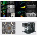
1783545296814.png1783545225071.png


Looking beyond traditional sensing applications, Lingming is aggressively positioning itself in the critical infrastructure of AI computing: optical interconnects. Recognizing that data transmission is a new bottleneck for exploding AI compute power, the company is adapting its proven "array technology" from laser radars to create high-density optical chips capable of delivering up to 40Tbps total bandwidth with ultra-low energy consumption. Supported by a joint research project selected for China's National Key R&D Program and partnerships with Tsinghua University, Lingming plans to move from prototype development in 2026 to mass production by 2028, effectively tackling the power and space limitations of traditional data center networking.

This strategic evolution is further solidified through deep ecosystem integration rather than simple component sales. The partnership with Zhiyang Innovation includes a commitment to joint R&D, allowing Lingming to co-design specialized chips for complex industry scenarios like smart inspections while leveraging the investor's supply chain capabilities. With revenue surpassing 1 billion RMB and losses rapidly declining in recent years, Lingming has successfully transitioned from a technology startup to a scalable system-level solution provider, poised to become a cornerstone of China's AI photonics infrastructure through its dual focus on next-generation sensing and high-speed data transmission.

Please, Log in or Register to view URLs content!
 

tokenanalyst

Lieutenant General
Registered Member

Tongji University’s "Nano-Ruler" tech wins China’s top prize​


Interesting this project is already commercialized.

Yuwei Semiconductor, as the second participating unit, won the first prize of the National Science and Technology Progress Award for its project "Key Technologies for Nanoscale Metrology of Quantum Optical Lattice Constants and Their Application in Integrated Circuits ." This project was led by Tongji University , with Yuwei Semiconductor collaborating with the National Institute of Metrology, Guilin University of Electronic Technology, and the Shanghai Institute of Metrology and Testing Technology, among others . After more than twenty years of dedicated research, the project team manufactured a series of national first-class standard materials for nanoscale lengths and angles, providing a "precise ruler" for instrument calibration and standardization in the field of nano-manufacturing such as integrated circuits.
uwei has long been deeply involved in the field of measurement and testing equipment and has a long-term need for high-precision technology. The promotion and application of this technology provides a basic technology for accurate measurement in nano-manufacturing and other fields. It can not only help with the design of standard sheets, but also test and use standard sheets, shorten the nano-metrology transfer chain, improve the flatness level, and is more suitable for solving industrial application problems.

Key technologies of nanometer metrology and their applications in integrated circuits

1783547029277.png

Please, Log in or Register to view URLs content!
 

GulfLander

Brigadier
Registered Member

Apple begins testing CXMT chips for devices sold in China, FT says​

  • Apple has reportedly begun testing DRAM chips from China's state-backed ChangXin Memory Technologies for devices sold within China.
  • It is lobbying the U.S government to permit broader use of its products, the Financial Times reported on Wednesday, citing people familiar with the matter.
Please, Log in or Register to view URLs content!

...

Please, Log in or Register to view URLs content!
 

tokenanalyst

Lieutenant General
Registered Member

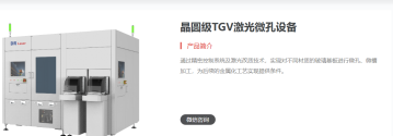
Di'er Laser achieved overseas sales of its TGV equipment in 2026.​


In 2026, the company's TGV equipment achieved overseas sales, and there were also small-batch repurchase orders. Please continue to pay attention to the company's periodic reports for the contribution of TGV equipment to revenue in 2026! Benefiting from the company's application of ultrafast lasers in the photovoltaic industry, the company has a deep technical accumulation in the application of ultrafast lasers, and can actively respond to customers' process needs, meeting their efficiency and yield requirements.

1783609127004.png

Please, Log in or Register to view URLs content!
 
Top