Chinese semiconductor thread II

tokenanalyst

Lieutenant General
Registered Member

Hubei Xingchen completes over 4 billion yuan Series A financing, the largest single financing in China's advanced packaging industry this year, landing in Optics Valley.​


Hubei Xingchen Technology Co., Ltd., based in Wuhan’s Optics Valley, has successfully completed a Series A financing round exceeding 4 billion yuan, marking the largest single investment in China’s advanced packaging industry this year. Backed by leading domestic semiconductor investors, the capital will accelerate R&D and pilot production capabilities focused on the company’s proprietary 3D heterogeneous integration technology. This innovation significantly enhances memory bandwidth and reduces storage latency for AI computing clusters and smart terminals, addressing critical chip performance bottlenecks while demonstrating strong market confidence in advanced packaging as a strategic pathway to overcoming semiconductor constraints and driving China’s tech self-reliance.

The funding directly supports the imminent commissioning of Hubei Xingchen’s Phase II pilot production line by September 2026, bringing total project investments beyond 7 billion yuan with a planned monthly capacity of 20,000 wafers. Originating from Jiangcheng Laboratory technology transfers, the company operates as a neutral open platform that provides high-density packaging R&D and domestic equipment/material verification services without engaging in mass terminal chip production. By scaling collaborative testing across the supply chain and strengthening Wuhan’s semiconductor ecosystem, Hubei Xingchen is positioned to bridge key gaps in high-end packaging verification and accelerate the independent, controllable development of China’s integrated circuit industry.

Please, Log in or Register to view URLs content!
 

tokenanalyst

Lieutenant General
Registered Member

Shenzhen Pinghu Laboratory and China Electronics Technology Group Corporation (CETC) signed a framework cooperation agreement on Electron Beam Lithography machines.​


Shenzhen Pinghu Laboratory and the China Electronics Technology Group Corporation (CETC) have announced a major breakthrough in the pilot testing of China’s first domestically produced, production-ready electron beam lithography (EBL) machine. After extensive iterative optimization and joint engineering efforts by CETC Electronic Equipment Group and CETC Research Institute No. 48, the equipment has successfully cleared production-line-level verification. Its performance, stability, and process capabilities now meet industrial manufacturing standards, marking a pivotal step in localizing high-end lithography tools and reinforcing China’s semiconductor supply chain independence.

The announcement was accompanied by a framework cooperation agreement signing ceremony at the Shenzhen Pinghu Laboratory. Prior to the formal proceedings, attendees toured the laboratory’s exhibition hall and cleanroom facilities to review its research infrastructure and pilot-scale verification capabilities. CETC equipment expert Fan Jianghua outlined the machine’s core technological breakthroughs, while lab lithography manager Yan Qiushi presented detailed findings from a three-year, full-process pilot testing program. Both sides also conducted in-depth discussions on technical bottlenecks, verification methodologies, and industrial deployment pathways.

Laboratory Director Wan Yuxi highlighted the facility’s mission to serve as a national pilot-scale platform for validating and commercializing domestic semiconductor equipment. Wang Ping, Chairman of CETC Electronic Equipment Group, stressed that central enterprises will continue to prioritize core technology self-reliance through deep industry-academia collaboration. Formalizing their partnership, Jia Guojun of Shenzhen Pinghu Laboratory and Sun Yong of CETC Institute No. 48 signed a cooperation framework agreement focusing on five key areas: equipment iteration, process advancement, talent cultivation, technology transfer, and joint patent development.

This achievement bridges a critical gap in the engineering application of domestically manufactured EBL systems, directly challenging long-standing foreign monopolies in micro-nano fabrication, photomask production, quantum chips, and advanced compound semiconductors. Shenzhen Pinghu Laboratory, which has already completed production-line verification for 124 sets of domestic equipment through its open public platform, will continue to accelerate the industrialization of independent semiconductor technologies. Moving forward, the partnership aims to expand joint R&D, streamline commercialization channels, and deliver a complete suite of domestically developed lithography tools to support the high-quality advancement of China’s integrated circuit industry.

Please, Log in or Register to view URLs content!
 

tokenanalyst

Lieutenant General
Registered Member
Allwinner and Rockchip are having a good year. My theory is that the AI bubble is pushing people to buy ARM devices for home entertainment because are lower priced than Intel-AMD devices

Allwinner Technology: Net profit is expected to increase by 195%-220% year-on-year in the first half of the year.​


Allwinner Technology announced that it expects its net profit attributable to shareholders of the listed company for the first half of 2026 to be between RMB 475 million and RMB 515 million, representing a year-on-year increase of 194.73% to 219.55%. During the reporting period, in response to rising costs of upstream raw materials and packaging, such as those for storage, the company raised its product sales prices. Simultaneously, the company actively expanded its business across various product lines and promoted the mass production of new products, resulting in a year-on-year increase of approximately 40% in operating revenue, which in turn drove the growth in net profit. The company continued to increase its R&D investment, with R&D expenses increasing by more than 20% year-on-year. The company expects non-recurring gains and losses to have an impact of RMB 33 million to RMB 37 million on net profit. Note: The company's Q2 net profit is expected to be RMB 272 million to RMB 312 million, and Q1 net profit was RMB 203 million. Based on this, Q2 net profit is expected to increase by 33% to 53% quarter-on-quarter.​

Rockchip: First-half net profit may surge 71.33%​

Rockchip Electronics, a domestic chip manufacturer, released its 2026 interim results forecast. It expects to achieve operating revenue of RMB 2.87 billion to RMB 2.91 billion in the first half of the year, an increase of RMB 824.16 million to RMB 864.16 million, representing a year-on-year growth of 40.28% to 42.24%.

Please, Log in or Register to view URLs content!
 

tokenanalyst

Lieutenant General
Registered Member

Allwinner A537/A333 Android AIoT Product Package Released, Creating Four New Smart Commercial Display Solutions​


To accurately match the differentiated needs of various application scenarios for Android solutions, Allwinner Technology officially launched the new A537/A333 Android AIoT product package. This product package integrates the chip's rich display interface support and built-in AI algorithm capabilities, which can meet the requirements of application scenarios such as advertising displays, cash registers, karaoke machines, and ArmPCs, and build a smart commercial display platform solution with wide coverage, flexible deployment and high efficiency for industry customers.

The Allwinner A537/A333 is a chip product supporting the Android system, designed for the tablet and related tablet markets. It integrates Arm® Cortex® - A73 and Arm Cortex-A53 CPUs and a Mali™-G57 MC1 GPU, meeting the high-performance computing requirements of the GMS LCO policy. It has joined Google's GRF program and is EDLA certified. For storage, it supports multiple specifications including DDR3, DDR3L, LPDDR3, DDR4 , LPDDR4 , and LPDDR4x, and features H.265/H.264/VP9 hardware decoding and H.264 hardware encoding capabilities. It supports a rich array of peripheral interfaces, including high-speed interfaces such as PCIe 2.1, USB 3.1 Gen1 DRD, and GMAC, as well as display output interfaces such as RGB, Dual LVDS, MIPI DSI, eDP 1.3, and E-ink, and supports dual-screen display functionality.

A537: Mid-to-high-end octa-core tablet chip
  • Dual-core A73 + six-core A53 big.LITTLE architecture​
  • Up to 16GB DDR, 4CS chip select and compatible with 64-bit DRAM​
  • Supports up to 2K@60fps display​
A333: Affordable Five-Core Tablet Chip
  • Single-core A73 + quad-core A53 big.LITTLE architecture​
  • Up to 8GB DDR, 4CS chip select and compatible with 64-bit DRAM​
  • Supports up to 1080P@60fps display​
  • A333 and A537 can be replaced via P2P.​

Please, Log in or Register to view URLs content!
 

tokenanalyst

Lieutenant General
Registered Member

China's first 2D semiconductor demonstration process line has been completed in Shanghai, contributing to the city's efforts to build an industrial hub.​


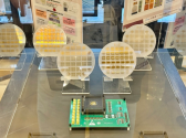
Yuanji Microelectronics (formerly Jiwei Technology) officially commissioned China’s first eight-inch two-dimensional semiconductor engineering demonstration process line in Shanghai’s Pudong New Area, marking a decisive transition of advanced chip materials from academic research to industrial production. The fully operational pilot facility houses integrated lithography and etching systems currently undergoing continuous stability debugging, establishing a complete engineering chain that spans from material preparation to chip integration. This milestone confirms that China’s two-dimensional semiconductor technology has successfully moved beyond the laboratory phase and entered rigorous engineering verification and small-batch tape-out stages, laying the groundwork for standardized industrial design.

Two-dimensional semiconductors are increasingly viewed as a viable pathway beyond Moore’s Law, particularly as conventional silicon manufacturing approaches its physical limits around the two-nanometer node. Atomically flat materials such as molybdenum disulfide and tungsten diselenide provide superior gate control at short-channel scales and significantly simplify fabrication by eliminating complex three-dimensional nanoscale steps. Building on this advantage, Yuanji Microelectronics announced that it will utilize the newly commissioned eight-inch platform in the second half of 2026 to develop a process path equivalent to the silicon-based ninety-nanometer node. Alongside this roadmap, the company launched its foundry tape-out services and released version 0.1 of a five-hundred-nanometer Process Design Kit (PDK). Fully compatible with mainstream EDA toolchains and achieving a yield exceeding 99.99 percent, this PDK breaks international performance records for two-dimensional semiconductors and will support circuit designs scaling to hundreds of thousands of transistors.

The company’s strategic vision targets a broad spectrum of commercial applications across memory, analog, logic, and next-generation computing fields. Leveraging the ultra-low leakage current characteristics of 2D materials, Yuanji plans to initially deploy its technology in edge-side and high-compute DRAM architectures, where reduced refresh power consumption offers significant efficiency gains. Beyond memory, the platform holds strong potential for radio-frequency analog circuits, radiation-hardened communications, brain-computer interfaces, optoelectronic sensing, and quantum computing. To accelerate industry adoption, Yuanji will also advance heterogeneous integration by bonding two-dimensional semiconductors with traditional silicon chips using advanced packaging techniques, gradually building a design and manufacturing ecosystem for two-and-a-half-dimensional and quasi-three-dimensional integrated circuits.

This industrial breakthrough is strongly supported by Shanghai’s strategic initiative to establish a globally competitive hub for atomic-level chip manufacturing. Municipal authorities have prioritized two-dimensional semiconductors as a key future growth industry, focusing on wafer-level material R&D, collaborative innovation platforms, and full-chain ecosystem development that bridges research, pilot production, and mass manufacturing. The project has attracted substantial capital, beginning with a one-hundred-million-renminbi angel round in December 2025 and followed by investments from Saiwei Electronics, Huakong Fund, Pudong Fund, and Guokai Kechuang. Strategic partnerships have also been formalized with leading academic institutions, including Peking University, Tsinghua University, Shanghai Jiao Tong University, and Nanjing University, to open university-led foundry services. Additionally, industry agreements with Xi’an Pioneer Institute and Shanghai 2D Star Technology will enable process platform sharing, technology transfer, and joint ecosystem development.

The rapid progression of the pilot line from initial activation earlier this year to full operational status—demonstrates a highly effective model of collaborative innovation among government agencies, universities, venture capital, and semiconductor enterprises. With sustained support in funding, equipment optimization, and supply chain integration, Yuanji Microelectronics is positioned to guide two-dimensional semiconductors from engineering validation toward high-yield manufacturing. As the industry shifts from prototype development to standardized industrial design, Shanghai’s emerging cluster is well underway to become a central driver in shaping the global landscape of post-silicon semiconductor technology.
1783617596199.png

Please, Log in or Register to view URLs content!
 

tokenanalyst

Lieutenant General
Registered Member

Yuemo Advanced has successfully prototyped an ultra-large-size all-glass 2.5D in-memory computing package.​

With the increasing demand for computing power and low power consumption in AI chips, advanced packaging has become a key technological path to overcome the physical bottlenecks of Moore's Law.

1783620450248.png

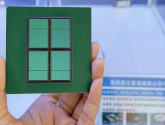
Recently, Yuemo Advanced has completed the prototype production of its ultra-large-size in-memory computing 2.5D packaging solution based on glass substrate and glass interposer. The product can be widely used in high-precision fields such as AI computing clusters, autonomous driving, high-performance supercomputing, and aerospace.

Features
  • Heterogeneous integrated architecture: It adopts a 2.5D advanced packaging architecture with a single package substrate and four glass interposers, integrating four logic chips and four memory chips to achieve heterogeneous integration of logic and memory chips for in-memory computing; the number of packaged micro bumps is nearly 50,000, supporting ultra-high density signal interconnection and perfectly adapting to the ultra-high bandwidth data transmission scenarios of in-memory computing chips.​
  • Extra-large size: The overall package size is 75×75mm², and the effective chip area accounts for more than 40% of the total package area, which greatly improves the chip integration density under large-size packaging;​
  • Ultra-low warpage: Relying on the excellent dimensional stability and thermal expansion matching characteristics of the glass substrate, the overall warpage of the package is only 67μm, which is 80.85% lower than that of organic substrate solutions, and the product reliability has been verified.​
  • Lightweight advantages: Compared with traditional organic substrate packaging solutions, the all-glass 2.5D solution reduces the overall weight by 40% and the core thickness by more than 50%, making it more suitable for the lightweight assembly requirements of end products.​
The all-glass 2.5D packaging technology solution has significant technical advantages in four dimensions: molding size, structural stability, warpage control, and lightweighting.

Please, Log in or Register to view URLs content!
 

tokenanalyst

Lieutenant General
Registered Member

The expansion projects of Qingyuan Yuanchuang Precision Zirconia, Large Plate Alumina, and Silicon Carbide Focusing Rings are about to enter mass production.​


The expansion project for Qingyuan Yuanchuang Precision (a subsidiary of Lead Technology Group) in Qingyuan High-tech Zone has completed factory construction and equipment installation. It is ahead of schedule, with main production lines expected to begin mass production in October 2026.
The facility produces critical semiconductor manufacturing components, including:
  • MFC (Gas Mass Flow Controllers)​
  • Chambers​
  • Zirconia (Zirconium Oxide)​
  • Large-plate Alumina​
  • Silicon Carbide Focusing Rings​
Once at full production, the project is projected to generate an annual output value of 236 million yuan, strengthening Qingyuan's semiconductor new materials industry. The expansion addresses urgent demand for domestically produced core semiconductor components, aiming to resolve industry "bottleneck" shortages driven by growth in the semiconductor and AI sectors. Established in July 2024, Qingyuan Yuanchuang Precision focuses on domestic substitution of semiconductor components. It has already entered the global top-tier supply chain and supplies leading domestic manufacturers like AMEC, with technology comparable to international leaders.

Please, Log in or Register to view URLs content!
 
Top