Some are even switching to their own ASICs, this could be like crypto hardware all over again.Chinese Firms Leave Nvidia for Local AI Suppliers, Survey Shows

You are using an out of date browser. It may not display this or other websites correctly.
You should upgrade or use an alternative browser.
You should upgrade or use an alternative browser.
Chinese semiconductor thread II
- Thread starter vincent
- Start date
XinGen Technology and NIO signed a strategic cooperation agreement to jointly build a joint laboratory for automotive-grade power semiconductors.
Silicon Carbide (SiC) power semiconductor manufacturer XinGen Technology and electric vehicle giant NIO signed a strategic cooperation agreement in Wuxi to jointly establish a "Joint Laboratory for Automotive-Grade Power Semiconductors." This partnership marks a significant shift from simple device supply to deep collaborative innovation, aiming to accelerate the development of high-voltage architectures, specifically targeting NIO's transition to 900V systems. By leveraging XinGen's location in the Wuxi Xidong New City Business District and its Test and Application Center (NTAC), the two companies plan to create an integrated R&D ecosystem that covers the entire vehicle chain—from chip design through modules, electric drives, and final vehicle application—to ensure superior product quality and performance.
The newly formed joint laboratory will serve as a core platform for technological advancement, focusing on testing verification, reliability research, and forward-looking technology development within a closed-loop system. Utilizing NTAC's comprehensive one-stop services, which include performance testing, aging screening, big data analysis, and failure analysis, the lab will provide solid technical support for NIO's evolving electric drive systems while simultaneously empowering XinGen to assist in the iterative upgrade of its partners' platforms. This collaborative infrastructure is designed to streamline the path from technology research to mass production applications, fostering a robust industrial ecosystem that benefits both OEMs and domestic power semiconductor providers.
Strategically, this agreement positions NIO as it seeks to strengthen its domestic supply chain for critical automotive components while moving up the value chain with leading Chinese manufacturers. For XinGen Technology, entering NIO's deep partner industrial chain validates its capabilities in advanced SiC technology and opens doors for full-range product delivery including chips, modules, and system-level solutions. Together, these entities aim to promote high-quality development in China's new energy vehicle sector by jointly driving the independent control and innovation of core components, setting a benchmark for future OEM-supplier collaborations in the rapidly evolving electric mobility landscape.

quiet battle playing in the background of China/Japan resource battle in the production of InP chips and substrate. China is cutting of Indium to Japan and Japan is cutting off Phosphorus to China, but it appears that China has now developed domestic supply chain for InP production.
China almost certainly made sure that they had domestic substitutes for every single Japanese import before instituting the recent rounds of formal export bans. That's probably one of the reasons why it took half a year from Takaichi's speech to the sanctions.China is cutting of Indium to Japan and Japan is cutting off Phosphorus to China, but it appears that China has now developed domestic supply chain for InP production.
Guangli Microelectronics creates 3D IC yield solutions to support the development of the Tao Law ecosystem.
In the post-Moore era, the semiconductor industry is embracing a new paradigm centered on Tao's Law, a time-scale theory that enables performance breakthroughs in HPC, AI computing, and automotive chips. This approach leverages advanced technologies such as:
- Logic Folding (reducing transistor counts per module),
- Ultra-narrow pitch hybrid bonding (<1.5μm),
- TSV multi-stack architectures,
- And sub-0.5μm alignment precision.
However, these advancements introduce significant yield and process challenges:
- Extreme hybrid bonding requirements: CMP (chemical-mechanical polishing) flatness control and <0.5μm overlay accuracy are critical; even ppm-level open defects can cause batch failures.
- Wafer-to-wafer parameter mismatch: Logic folding often combines wafers from different batches/nodes, amplifying timing variability and reducing timing margins.
- Testing bottlenecks for massive 3D chips: 64/96-core stacked dies face overcrowded DFT (Design-for-Test) routing, high test data volumes, expensive equipment needs, and incomplete fault coverage especially for automotive safety standards like ISO
To address these hurdles, Guangli Microengineering has developed an independently researched technology matrix spanning the entire chip lifecycle:
1. DFM Simulation & Hybrid Bonding Control (TQV)
1. DFM Simulation & Hybrid Bonding Control (TQV)
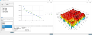
- CMP + Hybrid Bonding TQV: Combines advanced CMP simulation to predict surface defects with dedicated TQV test structures integrating millions of bonding pairs per die. This enables ppm-level open defect detection and reduces hybrid bonding iteration cycles by up to 50%.
2. Advanced Process Control (Adv-PCM)
- A next-generation wafer-level parameter control system offering:
- 100x faster testing than traditional PCM, with full-wafer parameter mapping;
- Monitoring of LPE effects, SRAM mismatch, ppm-level device anomalies, and AC oscillation performance;
- 10–1500x higher mask utilization;
- Integration of self-developed T4100S high-speed WAT (Wafer Acceptance Test) equipment for rapid data acquisition.
- Upcoming AI-driven wafer matching algorithms will auto-pair wafers with optimal parameter compatibility, mitigating inter-wafer variability.
3. 3D-Specific DFT Testing (QuanTest)
A comprehensive solution tailored for stacked chips:
A comprehensive solution tailored for stacked chips:
- SDS High-Speed Scan Bus: Each core features a local scan host, reducing top-tier DFT routing by 90% and cutting test time by 4x; ideal for HBM, large-scale heterogeneous SoCs, and 3D stacks.
- On-Chip Compare IP: Minimizes ATE (Automatic Test Equipment) pin requirements while supporting "Partial Good Die" yield scenarios with built-in failure diagnosis.
- ATPG + SAFA Fault Injection Fusion: Closes cross-asynchronous domain testing gaps to achieve >99% fault coverage compliant with ISO 26262, critical for automotive and AI chips.
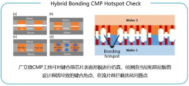
As Moore's Law slows, Tao's Law is driving the next generation of semiconductor integration. Guangli Microengineering's integrated "DFM simulation + high-density electrical testing IP + fast test equipment + AI-based yield platform + 3D DFT" stack addresses critical bottlenecks in:
- Chip design (via DFM tools),
- Manufacturing (process monitoring & bonding control),
- Testing (3D-specific DFT and high-speed WAT), and
- Packaging (hybrid bonding validation).
By providing domestic alternatives to foreign tools, Guangli Microengineering strengthens China's ability to scale 3D IC production for AI accelerators, HPC systems, and automotive electronics. This collaboration with industry partners underscores a broader ecosystem shift toward native Chinese innovation in advanced semiconductor architectures.
Interesting.
Hangzhou Yuzhiquan Precision Instruments Co., Ltd., in partnership with Zhejiang University's National Key Laboratory of Extreme Optics Technology and Instruments, has officially launched its "10,000-channel 3D Nano Laser Direct Writing Lithography Machine." This device represents a significant milestone for China's semiconductor and micro-nano manufacturing sectors.
Traditional two-photon laser direct writing technology is limited by "single-beam scanning," which struggles with large-area, high-efficiency production.
The company developed a 10,000-channel rapid independent control solution that generates over 10,000 independently controllable parallel laser focal points simultaneously and has an intelligent global optimization algorithm ensures light intensity uniformity exceeds 95%, overcoming the bottlenecks of older single-beam methods.
The new machine offers unprecedented speed and precision: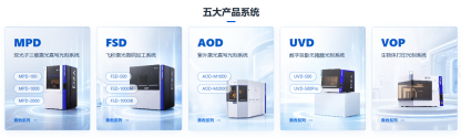
Yuzhiquan's "10,000-channel 3D nano laser direct writing lithography machine" has been officially launched!
Hangzhou Yuzhiquan Precision Instruments Co., Ltd., in partnership with Zhejiang University's National Key Laboratory of Extreme Optics Technology and Instruments, has officially launched its "10,000-channel 3D Nano Laser Direct Writing Lithography Machine." This device represents a significant milestone for China's semiconductor and micro-nano manufacturing sectors.
Traditional two-photon laser direct writing technology is limited by "single-beam scanning," which struggles with large-area, high-efficiency production.
The company developed a 10,000-channel rapid independent control solution that generates over 10,000 independently controllable parallel laser focal points simultaneously and has an intelligent global optimization algorithm ensures light intensity uniformity exceeds 95%, overcoming the bottlenecks of older single-beam methods.
The new machine offers unprecedented speed and precision:
- Printing Speed: Over 200 million voxels per second.
- Resolution: Minimum feature size capable of reaching sub-50nm.
- Scanning Efficiency: 2D surface scanning rates up to 40 square millimeters per minute (dozens of times faster than traditional methods).
- Capacity: Can fully cover a standard 12-inch wafer in one pass.
The machine provides critical support for several high-tech industries:
- Semiconductors & Manufacturing: Production of high-end photomasks, DOE masks (diffractive optical elements), and MEMS sensors.
- Photonic Chips: Supports rapid prototyping and small-batch development with complex 3D structures.
- Metasurfaces: Drastically reduces production time from weeks to hours for applications in AR/VR, LiDAR, and 6G communications. This is currently the first product category where the machine has been successfully implemented commercially.
Founded in December 2022 by senior researchers and entrepreneurs in Hangzhou, Yuzhiquan was established specifically to solve national bottlenecks in lithography technology. The collaboration with Zhejiang University underscores its focus on advanced optical precision instrument R&D.
The Andetop Chemical Hefei High-Purity Precursor and Electronic Solvent Project, with a total investment of 500 million yuan, broke ground.
The groundbreaking ceremony for Andetop Chemical (Anhui) Electronic Materials Co., Ltd.'s high-purity precursor and electronic-grade solvent project was held in Hefei's Xinqiao Integrated Circuit Science and Technology Park. This strategic initiative, a joint venture between the domestic leader Andetop Chemical and overseas partners, involves a total investment of 500 million yuan designed to construct advanced production lines for key chip manufacturing materials. The new company, established with a registered capital matching the project's investment scale under legal representative Wang Qiongyu, aims to fill critical gaps in Hefei's integrated circuit industry supply chain by producing essential upstream components that were previously reliant on foreign sources.
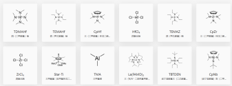
The parent entity, Anhui Andekeming Semiconductor Technology Co., Ltd., is a national-level "Little Giant" specializing in high-purity ALD/CVD precursors for advanced logic and memory chips, with existing products already supplied in batch to major domestic foundries like SMIC and Changxin Memory. The new facility covers nearly 100 acres and will establish an intelligent production line encompassing synthesis, purification, packaging, and solvent manufacturing, targeting completion by 2027. Once operational, the plant will provide large-scale supplies of metal precursors and ultra-high-purity electronic solvents for logic chips, memory devices, and advanced packaging, while Andekeming continues to develop its own liquid delivery equipment to offer integrated "materials plus equipment" solutions.
From an industry perspective, this project represents a crucial step toward reducing domestic reliance on overseas monopolies for strategic semiconductor consumables used in atomic-level thin-film deposition and wafer cleaning processes. By leveraging Hefei's mature chip manufacturing cluster, the facility will shorten delivery cycles for local fabs and packaging firms while promoting regional self-sufficiency in upstream materials. Chairman Wang Qiongyu emphasized that this joint venture is pivotal not only for meeting surging domestic demand but also for positioning Andetop as a global supplier through export-oriented production, thereby strengthening Hefei's status as a major domestic manufacturing center for advanced electronic materials.
The world's first 6/8-inch gallium oxide production line has started mass production in Hangzhou.
Gallium oxide is considered an important representative material of fourth-generation semiconductors, with advantages such as ultra-wide bandgap and high breakdown electric field. It has broad application prospects in fields such as new energy vehicles, smart grids, photovoltaic energy storage, rail transportation, AI computing centers, commercial aerospace and defense.
In crystal growth, the company has independently developed the world's first casting crystal growth technology, which can stably grow ultra-thick gallium oxide single crystals. Combined with its proprietary ultra-thin substrate processing technology, this increases the substrate yield per crystal block to 3 to 4 times the original amount. At the same time, this process significantly reduces the amount of precious metal iridium used, reducing substrate manufacturing costs by more than 80%.
In epitaxial manufacturing, Gallium Core Semiconductor has developed a dedicated MOCVD epitaxial process for 6-inch (100) plane gallium oxide substrates, becoming the world's first company to achieve commercial supply of 6-inch homoepitaxial wafers. The homoepitaxial wafers it produces have an epitaxial layer thickness of more than 10 micrometers, excellent film thickness uniformity, and thickness variance controlled within 1%.
In crystal growth, the company has independently developed the world's first casting crystal growth technology, which can stably grow ultra-thick gallium oxide single crystals. Combined with its proprietary ultra-thin substrate processing technology, this increases the substrate yield per crystal block to 3 to 4 times the original amount. At the same time, this process significantly reduces the amount of precious metal iridium used, reducing substrate manufacturing costs by more than 80%.
In epitaxial manufacturing, Gallium Core Semiconductor has developed a dedicated MOCVD epitaxial process for 6-inch (100) plane gallium oxide substrates, becoming the world's first company to achieve commercial supply of 6-inch homoepitaxial wafers. The homoepitaxial wafers it produces have an epitaxial layer thickness of more than 10 micrometers, excellent film thickness uniformity, and thickness variance controlled within 1%.
Zhongjie Times has released a domestically produced six-axis MEMS inertial measurement unit that combines high reliability with high cost-effectiveness.
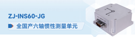
Beijing Zhongjie Times Aviation Technology Co., Ltd. has launched its domestically produced six-axis Micro-Electro-Mechanical Systems (MEMS) Inertial Measurement Unit (IMU), model ZJ-INS60-JG.
The unit follows the "SWaP-C" principle (Size, Weight, Power, and Cost), aiming to balance performance with affordability. Zhongjie Times adheres to a complete domestic supply chain for core sensor technology, covering everything from wafer fabrication through device creation, module assembly, algorithm development, and system integration.
- Performance Metrics:
- Features calibration across the entire temperature range.
- Offers high precision, large dynamic range, and strong resistance to shock/vibration.
- Gyroscope: Zero-bias stability better than 3°/h.
- Accelerometer: Zero-bias stability better than 100μg.
Designed for diverse needs including missile-borne systems, vehicle navigation, unmanned platforms, stabilization platforms, and industrial sensors. It is positioned as a solution for domestic substitution of core inertial navigation components.
Founded in 2006, the company has evolved over two decades from providing satellite navigation products to becoming a leader in integrated high-end navigation combining satellite, inertial systems, and intelligent algorithms. Is a National High-Tech Enterprise, Beijing Specialized & Innovative Enterprise, and a core member of Zhejiang Weixing Group (one of China's top 500 private enterprises).
Zhongjie Times plans to continue its "zero-to-one" leap in high-reliability spatiotemporal sensing. Their strategy involves using military products as a foundation while expanding into civilian markets like the low-altitude economy, embodied intelligence, and autonomous driving over the next 20 years.
Founded in 2006, the company has evolved over two decades from providing satellite navigation products to becoming a leader in integrated high-end navigation combining satellite, inertial systems, and intelligent algorithms. Is a National High-Tech Enterprise, Beijing Specialized & Innovative Enterprise, and a core member of Zhejiang Weixing Group (one of China's top 500 private enterprises).
Zhongjie Times plans to continue its "zero-to-one" leap in high-reliability spatiotemporal sensing. Their strategy involves using military products as a foundation while expanding into civilian markets like the low-altitude economy, embodied intelligence, and autonomous driving over the next 20 years.
The dual-line layout of 6-inch indium phosphide and 12-inch silicon carbide accelerates the industrialization of functional crystals.
The Institute of Functional Crystals of Tianjin University of Technology and Tianjin Binhai High-tech Zone officially signed a strategic cooperation agreement to jointly build a "Functional Crystal Materials Achievement Industrialization Base ," marking the official entry of the university's scientific research achievements in the field of functional crystals into the industrialization implementation stage. This base will rely on the technological accumulation of the Institute of Functional Crystals of Tianjin University of Technology and Academician Wu Yicheng's team, focusing on the industrialization of next-generation semiconductor crystals and optoelectronic crystal materials.
The first project is a 6-inch indium phosphide (InP) single-crystal project . Indium phosphide is a crucial semiconductor material in high-speed optical communication, widely used in high-speed lasers, photodetectors, optical modules, and other devices. It forms the foundation for 800G, 1.6T, and even higher-speed optical interconnects in the future. With the continuous growth of data center computing power driven by AI large-scale model training, the demand for high-speed optical modules is rapidly increasing, bringing new development opportunities to the indium phosphide market. This project will focus on high-speed optical module applications in AI computing infrastructure and has already begun technical discussions with leading companies in the industry, laying the foundation for subsequent industrial applications.
Another key project is the 12-inch silicon carbide single crystal . Unlike the silicon carbide substrates used in traditional power devices, this project primarily targets optical-grade silicon carbide applications, focusing on emerging markets such as AR glasses waveguides and AI chip thermal packaging. In recent years, the application of high thermal conductivity silicon carbide materials in advanced packaging, thermal management, and consumer electronics optics has been continuously expanding, and the ability to fabricate large-size crystals has become an important area of competition in the industry. According to the plan, the project aims to achieve small-batch supply in 2026.