Chinese semiconductor thread II

tokenanalyst

Lieutenant General
Registered Member

Tianxin Microelectronics was recognized as a "New Little Dragon" enterprise in hard technology in Wuxi High-tech Zone in 2026.​


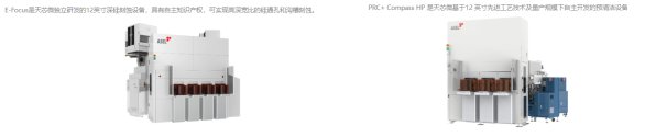
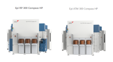
Jiangsu Tianxinwei Semiconductor Equipment Co., Ltd. was officially recognized as one of the second batch of "Hard Technology New Little Dragons" enterprises by Wuxi High-tech Zone. This prestigious honor came during the tenth National Science and Technology Workers Day, amidst a grand conference on the integration of technology, industry, and talent in Wuxi High-tech Zone. As part of only eight selected companies in this round, Tianxinwei earned its title through rigorous selection processes, highlighting its deep technical accumulation in critical semiconductor front-end processes specifically epitaxy and etching as well as its strong R&D capabilities and robust growth trajectory.

The "Hard Technology New Little Dragon" designation serves as an authoritative benchmark for nurturing new quality productive forces and constructing a modern industrial system within the zone. The selection criteria strictly evaluated candidates based on innovation levels in key sectors like artificial intelligence, low-altitude economy, advanced materials, and energy storage, while prioritizing technical barriers, R&D intensity, and growth rates. For Tianxinwei, this award is not merely an accolade but a powerful endorsement of its commitment to advancing semiconductor equipment technology. It provides the company with significant credibility as it continues to tackle core technologies, participate in national strategic initiatives, and integrate deeply into the broader regional industrial ecosystem.

Moving forward, leveraging the exclusive policy support, talent development opportunities, financial empowerment, and full-chain supply chain resources associated with this status, Tianxinwei is poised for accelerated expansion. The company plans to consolidate its innovative research framework by expanding its team, refining production processes, and optimizing product portfolios to achieve steady scaling and iteration in high-quality development. By steadfastly adhering to its initial mission of hard-core innovation, Tianxinwei aims to further enrich Wuxi High-tech Zone's integrated circuit industry landscape, contributing substantial creative energy to the region's pursuit of industrial high-quality growth and the cultivation of new forms of productive forces.
1783461047669.png1783461030884.png

Please, Log in or Register to view URLs content!
 

tphuang

General
Staff member
Super Moderator
VIP Professional
Registered Member
Please, Log in or Register to view URLs content!
Piotech news from today
日讯,拓荆科技董事长吕光泉今日在业绩会上表示,公司先进产品已进入规模化量产阶段,今年一季度毛利率回升,后续毛利率预计趋于平稳。未来公司将围绕先进制程需求,持续拓展薄膜沉积工艺覆盖面,并积极拓展三维集成领域产品。公司已全面覆盖PECVD、ALD等主流薄膜沉积设备,对应产品合计占据中国大陆薄膜沉积设备市场约50%份额,可触达的对应国内市场规模约46.5亿美元。公司2025年营收65.19亿元,占到自身可对接国内市场体量的20%左右,后续还有较大提升空间。 (科创板日报记者 吴旭光)

Please, Log in or Register to view URLs content!
BOE reporting on huge growth in profit
京东方A(000725.SZ)公告称,预计2026年半年度归属于上市公司股东的净利润为50.00亿元-55.00亿元,同比增长54%-69%。报告期内,存储产品价格持续上涨使消费电子终端产品销量不同程度承压,但显示行业需求仍保持韧性,五大主流应用LCD面板出货量持续保持全球第一,高刷新率、高对比度、高分辨率等高端产品出货量持续增加,经营稳健。LCD业务业绩同比显著增长。柔性AMOLED方面,公司持续深化客户合作,重点推动LTPO等高端产品出货,上半年公司AMOLED产品出货超8,000万片,同比保持增长。此外,在第8.6代AMOLED产线量产后,公司将依托该产线的规模化产能与领先技术优势,持续推动中尺寸高端OLED产品升级,稳步提升公司柔性AMOLED业务整体竞争力。2026 年上半年归属于上市公司股东的净利润中预计非经常性损益的金额约20亿元,较上年同期增加。小财注:公司Q2净利润预计32.93亿-37.93亿,Q1净利润17.07亿,据此计算,Q2净利润预计环比增长92%-122%。

Please, Log in or Register to view URLs content!
MetaX has started mass delivery of MXC600 and it's apparently fully booked until next year for some products
【沐曦股份孙国梁:部分产品订单已排到明年甚至之后, MXC600芯片系列已大规模出货】《科创板日报》8日讯,在“活力中国调研行”上海站中,沐曦股份首席产品官、高级副总裁孙国梁透露,公司部分产品订单已经排到明年甚至之后。MXC600芯片系列是公司今年主力,目前已经大规模出货。面对市场上“一卡难求”和“算力过剩担忧”的矛盾,他认为,目前通用、易用、稳定、可靠的算力是稀缺的,甚至是一卡难求,过剩的算力是指:适用一些不通用的架构、只能跑上一代模型或者某些细分类型模型等算力,是有一定的过剩。
 

tokenanalyst

Lieutenant General
Registered Member

Vertically Stacked Indium Gallium Zinc Oxide-Based Three-Dimensional Integrated Circuits.​

Abstract​

Monolithic three-dimensional (M3D) integration is a promising solution for next-generation integrated circuits, offering enhanced signal propagation, high integration density, and lower fabrication costs than planar architectures. Amorphous oxide semiconductors, with room-temperature deposition capability and large-scale uniformity, are well-suited for 3D applications, yet developing multitier high-performance oxide transistors compatible with traditional technologies remains challenging. Here, we present a threshold voltage modulation strategy for indium gallium zinc oxide (IGZO) transistors via channel thickness control and atomic-layer-deposited surface modification. A four-tier vertically stacked IGZO transistor array has been manufactured with sequential layer-by-layer integration; optimized transistors across the tiers exhibited a low subthreshold swing of 150 mV/dec and an on/off ratio exceeding 108. Combined with via-hole interconnects, we demonstrated functional computing-in-memory 3D circuits featuring inverter modules (tier 1–2) and dynamic random access memory (DRAM) components (tier 3–4). The work advances oxide semiconductors’ applications in future advanced 3D circuits.

1783522344534.png

Please, Log in or Register to view URLs content!
 

tokenanalyst

Lieutenant General
Registered Member
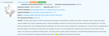
looks like the company is working in vacuum loaders. in this case EUV.

A vacuum plate transfer device​


summary
This utility model relates to the field of semiconductor technology, and in particular to a vacuum wafer transfer device, comprising a cavity, a first chamber and a second chamber disposed within the cavity, a heating component installed in the first chamber, a cooling component installed in the second chamber, and a transfer cavity. The first chamber and the second chamber are respectively connected to the transfer cavity. A robotic arm is disposed within the transfer cavity, and the robotic arm is used to transfer the wafer between the first chamber and the second chamber. The first chamber, the second chamber, and the transfer cavity are all connected to a vacuum pump. This utility model avoids wafer contamination or temperature fluctuations caused by immediate cooling after high-temperature injection within the same cavity, and avoids stress generation. By alternately achieving heating and cooling, it effectively utilizes the cavity space, facilitates increased production capacity, improves production efficiency, and meets the needs of large-scale production.​
1783522487836.png

A TM cavity vacuum transmission device​


summary
This utility model relates to the field of semiconductor technology, and in particular to a TM cavity vacuum transfer device, comprising a transfer cavity and several process cavities connected to the transfer cavity. The process cavities are respectively disposed around the periphery of the transfer cavity and connected to the transfer cavity via gate valves. A robotic arm for transferring photomasks is installed inside the transfer cavity. The process cavities include loading/unloading cavities, at least one process cavity, a calibration cavity, and a buffer cavity connected to the transfer cavity. The loading/unloading cavities are used for loading and unloading photomasks. A filling/discharging assembly is installed in the loading/unloading cavities to adjust the filling and discharging rates within the loading/unloading cavities to avoid flow field disturbances. This utility model avoids flow field disturbances, ensures constant pressure and flow field within the loading/unloading cavities, facilitates the formation of steady-state airflow, maintains pattern accuracy, and improves product yield.​

1783522707846.png
 

tokenanalyst

Lieutenant General
Registered Member

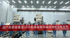
First domestic breakthrough! Jiangsu Zhixinda ships silicon-based display IZO low-temperature, low-damage magnetron sputtering equipment.​


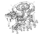
Jiangsu Zhixinda Technology Co., Ltd. has successfully shipped its first domestically produced silicon-based display IZO low-temperature, low-damage magnetron sputtering equipment. This marks a significant milestone for China's silicon-based Micro OLED industry, specifically for applications in AR/VR and automotive near-eye displays.

The shipment completely breaks the long-standing foreign monopoly on core coating equipment required for silicon-based Micro OLED mass production lines. Silicon-based Micro OLEDs are extremely sensitive to heat; traditional imported equipment often damages these delicate organic layers due to high temperatures and energetic particle bombardment, leading to low yields and short lifespans. Zhixinda's new equipment solves this by maintaining substrate temperatures between 40–60°C.

1783524228989.png

The machine features proprietary technologies including:​
  • Stable low-temperature control to protect organic films.​
  • Specialized target structures ensuring film uniformity errors within ±2%.​
  • Nanometer-level precision in coating thickness.​
  • Full domestic supply chain for core components (magnetron cathode, cavity, vacuum systems, etc.), eliminating reliance on overseas suppliers.​
The deployment of this equipment provides Chinese near-eye display manufacturers with a cost-effective and self-controllable process solution. By reducing procurement and maintenance costs while improving mass production yield, it accelerates the localization of China's entire AR/VR and automotive silicon-based display industry chain. Wu Zhehao, General Manager of Jiangsu Zhixinda, confirmed that the company plans to continue investing in R&D for iterative improvements in high-end vacuum coating equipment, aiming to promote large-scale production capabilities to empower the domestic new display sector's innovative development.

Please, Log in or Register to view URLs content!
 
Top