Chinese semiconductor thread II

tokenanalyst

Brigadier
Registered Member
Not to throw cold water on this: "it is pretty clear that there is already, not a immersion machine for 28nm process but for a 14nm process already working and patterning wafers.", but there have been comments by others that chips have microscopic engravings that indicate what lithography machine was used. Wouldn't domestic 14 nm chips be easily identifiable?
The overlay markings. If survive the cutting process.

SMEE trademark uDBO overlay mark, let see if techinsight find that one.
View attachment 146333


View attachment 146332
 

tokenanalyst

Brigadier
Registered Member
The overlay markings. If survive the cutting process.
And you know is for advance manufacturing processes like SAQP immersion or EUV because the previous generation of overlay markings was based of technique called Image Based Overlay (IBO) which was good enough back them but now current semiconductor devices require tight overlay requirements and at least ASML has move on to Diffraction Based Overlay using diffraction gratings, KLA has moved to scatterometry-based overlay wich is basically the same thing they just want to market it differently.
 

LanceD23

Junior Member
Registered Member
According to this article, SMEE duv tool for 28NM is still not ready. I thought they released it in 2023. Did it get delayed?

If China is still stuck in 90NM machines then its not getting EUV in 10 years
When did Beijing SMIC has 14 nm production line? Even going to 7nm? It's a surprise to me.
 

tokenanalyst

Brigadier
Registered Member

Major breakthrough in China MLED equipment!​

The Guangdong University of Technology's provincial and ministerial co-construction National Key Laboratory of Precision Electronic Manufacturing Technology and Equipment reported a breakthrough. Professor Chen Xin/Chen Yun's team, together with industry leaders such as Suzhou Maxwin Technology Co., Ltd., has made major breakthroughs in the research and development of key core technologies and equipment in the field of Mini/MicroLED display. The relevant results have been industrialized and applied, helping my country's new display industry to develop with high quality.

As a new generation of display technology, Mini/Micro LED has the advantages of high brightness, high contrast, and low power consumption, which is in line with the "dual carbon" strategic orientation and has huge market potential in consumer electronics, high-end display and other fields. However, high-efficiency and high-yield chip mass transfer and bonding technology has long been the focus of international technology competition.

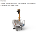
With the support of the "Intelligent Robot" project of the National Key R&D Program, the team of Guangdong University of Technology invented a new principle of two-dimensional high-frequency coordinated flying thorn crystals. Through the technical combination of "flying thorn crystals to increase speed, macro-micro composite to ensure accuracy, and directional compensation to increase yield", they built a full-chain independent technology system covering transfer methods, bonding processes, core components, and system control. In order to solve the problem of transferring Micro LEDs of smaller sizes, the team further broke through key technologies such as high-speed precision alignment, laser process coordination, and error compensation, and has obtained more than 20 invention patents in China and the United States.

Through in-depth industry-university-research cooperation with Suzhou Maxwin Technology Co., Ltd., a leading pan-semiconductor equipment company, scientific research results have been quickly transformed into real productivity. The flying thorn crystal mass transfer robot jointly developed by the two parties has achieved a leapfrog improvement in performance indicators and significantly reduced raw material consumption and manufacturing costs.

This equipment not only reaches the international leading level in technical indicators, but also realizes the batch shipment of Mini LED mass transfer production line, which is equipped with "Chinese core" for my country's display industry. At present, the relevant equipment has been applied on a large scale in commercial and consumer scenarios such as large-screen display, all-in-one conference machine, and home theater, promoting the upgrading of my country's high-definition display industry.

While making breakthroughs in Mini LED technology, the joint research team formed by Guangdong University of Technology and Maxwin Technology (Zhuhai) Co., Ltd., a subsidiary of Suzhou Maxwin Co., Ltd., has targeted the frontier field of Micro LED and achieved the localization of equipment such as laser stripping, giant transfer, bonding, and repair. The G3.5 generation line laser bonding equipment has been delivered to customers. The team pioneered a comprehensive solution for silicon-based Micro LED hybrid bonding wafer reconstruction, covering key equipment for the entire process such as wafer polishing, femtosecond laser cutting, plasma processing, and hybrid bonding. It integrates semiconductor integration technology with new display innovations, opening up a new path for large-scale mass production of ultra-high-definition displays.

Please, Log in or Register to view URLs content!
 

tokenanalyst

Brigadier
Registered Member

Jingsheng Co., Ltd. has achieved full coverage of key links in the preparation of silicon carbide materials​

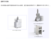
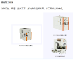
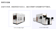
Jingsheng Co., Ltd.'s silicon carbide crystal growth equipment is one of its core businesses. The company has a keen insight into customers' core demands for "improving quality and reducing costs" of substrate materials, actively promoted the extension of the technology chain, and built a full-process equipment supply capability from:

-Silicon carbide powder synthesis.

1752685569036.png
-Crystal growth
1752685586900.png

-Ingot processing to epitaxial growth
1752685609113.png
-Epitaxial growth equipment

1752685624484.png


Please, Log in or Register to view URLs content!
 

tokenanalyst

Brigadier
Registered Member

Zhineng: First announcement of domestic silicon-based vertical GaN HEMT technology​


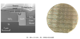
Guangdong Zhineng, attended the 15th International Conference on Nitride Semiconductors (ICNS-15) held in Sweden and gave an invited talk. The talk shared the team's original breakthroughs and application prospects in silicon-based vertical gallium nitride power devices (GaN HEMT) technology. The talk attracted heated discussions from international peers at the scene and after the meeting.

Guangdong Zhineng gave an invited speech at the ICNS conference It is understood that the widely used gallium nitride power devices currently mostly adopt a lateral structure, but in high-power, high-current scenarios they still face technical bottlenecks such as electric field management, device miniaturization and heat dissipation difficulties, making it difficult to fully utilize the performance advantages of gallium nitride materials.In contrast, the vertical GaN device architecture can break through the limitations of the lateral structure in conductivity (power density) and heat dissipation performance, demonstrating orders of magnitude of excellent performance and system integration potential. It is considered to be one of the key technical paths to promote GaN power devices to higher power.

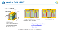
The Guangdong Zhineng team pioneered the world's first direct epitaxial growth of vertical GaN/AlGaN heterostructures and vertical two-dimensional electron gas channels (2DEG) on silicon substrates, and through precise process control, prepared gallium nitride fin structures with low dislocation density. This method has extremely high freedom in epitaxial structure design.

1752696261004.png

Based on this innovative platform, the team successfully developed the world's first normally-on device (D-mode VHEMT) with a vertical 2DEG channel and a normally-off device (E-mode VHEMT) with adjustable threshold voltage. In terms of process integration, the fully vertical electrode structure layout is achieved through the selective etching of source/gate electrodes and the complete removal of the silicon substrate, which can significantly improve the heat dissipation efficiency of the device. This innovative technology has extremely high mass production feasibility with the support of advanced process platforms, and also provides broad space for device miniaturization and high current performance iteration (power density).

At the same time, Guangdong Zhineng further demonstrated the world's first vertical two-dimensional electron gas gallium nitride power device structure, at which time the silicon substrate used for growth has not been removed. When the silicon substrate used for growth is removed, the observation surface is the original silicon substrate surface, and a complete vertical gallium nitride device wafer can be obtained.


1752696349938.png

Focusing on this original vertical GaN device architecture and process, Guangdong Zhineng has deployed a number of core intellectual property rights at home and abroad, formed a complete patent portfolio, and built a solid technical barrier. With continuous innovation in material epitaxy, structural design, and process integration, the vertical GaN power device platform is expected to become the key technology path for the next generation of high-performance GaN power devices.

Please, Log in or Register to view URLs content!
 

tokenanalyst

Brigadier
Registered Member

The world's first 8-inch GaN mass production IDM company will reach 20,000 pieces per month by the end of the year.​


As a global leader in GaN power semiconductors, Innoscience recently announced a major capacity expansion plan: its monthly capacity of 8-inch GaN wafers will increase from the current 13,000 to 20,000 by the end of the year, and plans to expand to 70,000 in the next five years, an increase of more than five times the current scale. This layout relies on the maturity of the company's 8-inch wafer manufacturing process and the continuous optimization of its yield rate - currently its wafer yield rate has exceeded 95%, significantly ahead of the industry average.
Please, Log in or Register to view URLs content!
 

huemens

Junior Member
Registered Member
China still 27% of revenues, and much more when counting the number of machines, because the most expensive EUV and immersion DUVi are banned in China.
Also note that not all of that is sales of machines. A significant portion of ASML revenue is maintenance. This quarter it's 27.25% (worldwide, they don't break it down by country). When there were no ArFi restrictions on China, China's share of overall revenue was much higher (about 50% in some quarters). China has a huge ASML installed base, so a significant portion of this and previous quarter's 27% figure is maintenance for existing machines.
 

tphuang

General
Staff member
Super Moderator
VIP Professional
Registered Member
Also note that not all of that is sales of machines. A significant portion of ASML revenue is maintenance. This quarter it's 27.25% (worldwide, they don't break it down by country). When there were no ArFi restrictions on China, China's share of overall revenue was much higher (about 50% in some quarters). China has a huge ASML installed base, so a significant portion of this and previous quarter's 27% figure is maintenance for existing machines.
Please don't write stuff like this without evidence to back it up. I don't ever recall China's overall share of revenue being 50%. In fact, even 40% from last year was quite abnormal and likely due to significant stocking up of higher end Arfi models that Dutch gov't gave licenses to.

Please, Log in or Register to view URLs content!
29% of ASML revenue in 2023 came from China
in 2022, this was 14%

There is in fact no reason why China's servicing/maintenance bill would be higher than 27% of overall, since historically speaking, its share of overall revenue is far less than 27%
 

tokenanalyst

Brigadier
Registered Member

China Micro's (AMEC) revenue in the first half of the year was 4.961 billion yuan, with net profit at the highest level, up 41.28% year-on-year​

China Micro Corporation released its 2025 semi-annual performance forecast, stating that the company expects its net profit attributable to shareholders of the parent company to reach 680 million to 730 million yuan in the first half of the year, a year-on-year increase of 31.61% to 41.28%, continuing the rapid growth trend in recent years.

On the basis of maintaining an average annual growth rate of more than 35% in operating income over the past 14 years, AMEC's operating income will continue to maintain rapid growth in the second quarter of 2025, with an estimated operating income of approximately RMB 2.787 billion, a year-on-year increase of approximately 51.26%. The estimated operating income for the first half of 2025 is approximately RMB 4.961 billion, a year-on-year increase of approximately 43.88%.

In terms of business, in the first half of the year, AMEC's etching equipment revenue reached 3.781 billion yuan, a year-on-year increase of 40.12%, and it is still the company's core growth engine; LPCVD thin film equipment revenue soared 608.19% to 199 million yuan, becoming a new growth highlight. The company said that its high-end etching equipment has achieved large-scale mass production in the key process links in the manufacture of advanced logic chips and memory chips, driving the company's performance to continue to rise.

As a leading company in the field of domestic semiconductor equipment, AMEC continues to increase its R&D investment. In the first half of 2025, the company's R&D investment reached 1.492 billion yuan, a year-on-year increase of 53.70%, accounting for 30.07% of its revenue, far exceeding the average level of companies listed on the Science and Technology Innovation Board (10%~15%).

Currently, the company's research projects cover six categories and more than 20 new devices, and the R&D cycle has been greatly shortened - it used to take 3 to 5 years to develop a new device, but now it only takes 2 years or even less. This means that in the next few years, AMEC is expected to launch more new products with market competitiveness and further consolidate its position in the industry.

Please, Log in or Register to view URLs content!
 
Top