Chinese semiconductor thread II

huemens

Junior Member
Registered Member
I don't ever recall China's overall share of revenue being 50%.
I wrote "about 50% in some quarters", it was actually 49% in some quarters. In 2024, both Q1 and Q2 were 49% and Q3 47%.
Please, Log in or Register to view URLs content!

China has gone through a lot of expansion and installed base is naturally going to be larger now than it was in 2022 and 2023.
 
Last edited:

tphuang

General
Staff member
Super Moderator
VIP Professional
Registered Member
I wrote "about 50% in some quarters", it was actually 49% in some quarters. In 2024, both Q1 and Q2 were 49% and Q3 47%.
Please, Log in or Register to view URLs content!

China has gone through a lot of expansion and installed base is naturally going to be larger now than it was in 2022 and 2023.
sure, that's because they were aggressively stocking up earlier last year. Those are purchases that otherwise would have a % spread over following quarters. For the full year, they were in the low 40s.

The machines purchased last year are unlikely to have all been installed by this point. Because again, they were stocking up machines. Machines that are brand new or haven't been installed don't need to be serviced. China as a % of servicing revenue for ASML is more likely to be based on 2018 to 2023 installations.

So you are on the whole making a really bad argument.
 

gelgoog

Lieutenant General
Registered Member
In a couple of years we could see another major expansion. SMIC, Hua Hong, YMTC, and CXMT have spare land at their existing fab sites they have not used yet. SMIC supposedly is running at 90% capacity so they probably could expand more.
 

tokenanalyst

Brigadier
Registered Member

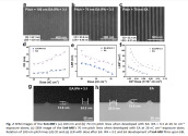
Hybrid Alkyl-Ligand Tin-oxo Clusters for Enhanced Lithographic Patterning Performance via Intramolecular Interactions.​

Abstract​

Tin-oxide clusters (TOCs) are promising candidates for next-generation extreme ultraviolet (EUV) photoresist materials due to their strong EUV absorption properties and small molecular sizes. The surface ligands are critical to the photolithographic patterning process; however, the precise regulatory mechanisms governing their functionality require further investigation. Building upon our previously reported Sn4-oxo clusters, Sn4-Me-C10 and Sn4-Bu-C10, which incorporate butyl and methyl groups, respectively, this study present the synthesis of a novel cluster, Sn4-MB, which integrates both butyl and methyl groups within the same Sn4-oxo core. This new compound demonstrates superior patterning performance compared to both Sn4-Me-C10 and Sn4-Bu-C10, as well as their mixed formulations. The enhanced performance is attributed to intramolecular interactions between the Sn-methyl and Sn-butyl groups in Sn4-MB, along with the generated radicals, which significantly mitigate energy transfer losses and reduce the distance of radical migration. In electron beam lithography (EBL) exposure experiments, optimization of the developer and reduction of film thickness allowed Sn4-MB to achieve lines with a critical dimension (CD) of 17 nm. Furthermore, during EUV exposure, Sn4-MB produced 75 nm pitch lines at a dose of 150 mJ cm-2, with a line CD of 33 nm. This study provides an effective molecular design strategy for enhancing the lithographic performance of TOC photoresists, highlighting their substantial potential for next-generation EUV lithography applications.

1752766798210.png

Please, Log in or Register to view URLs content!
 

tokenanalyst

Brigadier
Registered Member

The application advances of cordierite materials in photolithography.​

No. 52 Institute of China North Industry Group Corp., Ltd​

Abstract​

Cordierite has good application value in the field of lithography mobile platforms, because of the low thermal expansion, the high rigidity and low density. For EUV lithography machines, cordierite material design has been a key parameter for the material system of its operating platform. Although several manufacturers try to improve the performance of the lithography machines by adjusting the composition of cordierite or experimenting with various materials, the EUV lithography technology is only mastered by ASML, which leads to the high price of EUV lithography machines and the dependence on imports. In this paper, traditional and new lithography machine materials are provided and compared, the application of cordierite materials in lithography machine platforms is reviewed and evaluated, the status and the gap at home and abroad are analyzed and discussed. In the end, the paper provides more ideas for the development of the domestic lithography industry, gives better instructions to guide the trend of lithography machine research and promotes the development of lithography machines and chip industry at home.

Please, Log in or Register to view URLs content!
Cordierite - a key material for the development of photolithography machines

In the field of precision manufacturing in modern industry, cordierite has become a star material with its outstanding performance. Recently , Kyocera Corporation announced that its "precision cordierite" ceramic mirror has been selected for experimental equipment for optical communication between the International Space Station (ISS) and the mobile optical station on Earth. This high-performance ceramic not only has an extremely low thermal expansion coefficient, but also has excellent thermal shock resistance, good high-temperature stability and outstanding oxidation resistance. These characteristics make cordierite shine in many fields such as metallurgy, automobiles, catalysts, environmental protection, electronic packaging and infrared emission, especially in the field of semiconductor equipment manufacturing, showing great application potential, and is an ideal material for photolithography square mirrors, etc.
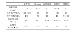
On the ultra-precision worktable of the lithography machine, the accuracy of the square mirror component is directly related to the resolution and production efficiency of the lithography machine. Its thermal expansion coefficient must be close to zero ( ≦2×10⁻⁸ K ⁻ ¹ ) to ensure that it can maintain extremely high positioning accuracy under temperature fluctuations. In addition, it must have high bending strength ( >190 MPa ) and high elastic modulus ( >140 GPa ), while maintaining low density to meet the needs of high-speed platform movement. Therefore, cordierite ceramics have become an ideal material for manufacturing square mirror components due to its extremely small expansion coefficient and excellent mechanical properties.

The chemical formula of cordierite is Mg₂Al₄Si₅O₁₈, which is the key ternary oxide in the MgO-SiO₂-Al₂O₃ system. Its theoretical density is about 2.6g·cm⁻³, and its melting point is about 1460℃. It has excellent properties such as good chemical stability, high resistivity (>10¹²Ω·cm), low dielectric constant (εr=6), and near-zero frequency temperature coefficient (τf=-32x10⁻⁶℃⁻¹). Its crystals have three structures, namely high-temperature stable phase α cordierite, low-temperature stable phase β cordierite, and low-temperature metastable μ cordierite. When the ambient temperature changes, the bond lengths of Al-O and Si-O remain almost unchanged, while the bond length of Mg-O increases significantly, providing more space for volume expansion. Therefore, cordierite exhibits a smaller thermal expansion coefficient in the C-axis direction, as low as 1.5x10⁻⁶K⁻¹~2x10⁻⁶K⁻¹ (25℃~800℃), maintaining extremely strong dimensional stability under temperature fluctuations, meeting the requirements of high-quality low thermal expansion materials.

Making cordierite powder into square mirror components is a complex process involving multiple steps. First, it is necessary to prepare high-purity, fine-particle-size, precisely proportioned, and evenly distributed cordierite powder, which is essential for sintering uniform and dense cordierite ceramics. Next, the powder will undergo a molding process to form the initial shape of the square mirror, such as dry pressing, isostatic pressing, or injection molding. By precisely controlling the pressure and mold design, a molded component with precise dimensions and regular shape can be obtained. The component is then sintered at high temperature to achieve densification and crystal phase transformation. The temperature, atmosphere, and time during the process are strictly controlled to ensure that the physical properties and microstructure of the product meet the requirements. Finally, the sintered square mirror components need to undergo precision machining and polishing to meet the requirements of surface roughness and geometric accuracy, so as to achieve the resolution and production efficiency required by the lithography machine.

In order to obtain ideal cordierite powder, existing methods include: solid phase sintering method, sol-gel method, molten glass method , etc. For example, the solid phase sintering method uses MgO, SiO2 , Al2O3 powders to mix by mechanical grinding in a ball mill or sand mill, but it is difficult to meet the material requirements of photolithography devices in terms of high purity maintenance, particle size control and multi-element mixing effect. The sol-gel method can prepare powders with fine particle size and uniform distribution, but the process is complicated and the production efficiency is low, which is not suitable for large-scale industrial production. The material obtained by the molten glass method has good homogenization effect and high purity, but the huge energy consumption leads to high production cost.
1752767382586.png

Please, Log in or Register to view URLs content!
 

tokenanalyst

Brigadier
Registered Member

Polytelluoxane as the ideal formulation for EUV photoresist.​

Key Lab of Organic Optoelectronics & Molecular Engineering, Department of Chemistry, Tsinghua University.

Abstract​

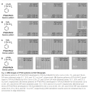
Extreme ultraviolet (EUV) lithography has become the essence of advanced semiconductor manufacturing processes. While enabling smaller feature sizes, EUV lithography imposes increasingly stringent requirements on the comprehensive performance and stochastic defect suppression of photoresist. The widely recognized strategy to minimize these defects is a material that integrates high EUV absorption and energy utilization into a homogeneous system based on molecular building blocks—the ideal formulation for EUV photoresist. However, achieving these integrated characteristics within a single molecule has remained an unresolved challenge. Here, we address all these requirements by polytelluoxane using an organic telluride monomer polymerized via Te─O bonds. This polymeric photoresist, operating through a main chain scission mechanism, demonstrates high-performance positive-tone lithography. Attributed to this ideal formulation, our photoresist achieves a comprehensive 18-nm line width at a dose of 13.1 mJ/cm2 with a line edge roughness of 1.97 nm. We believe that this strategy establishes a framework for the design of next-generation EUV photoresists.

1752769666986.png

Please, Log in or Register to view URLs content!
 

tokenanalyst

Brigadier
Registered Member

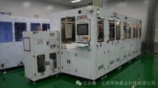
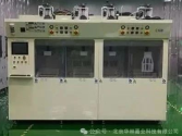
Silicon carbide special cleaning equipment delivered! Helping third-generation semiconductor customers achieve breakthroughs in mass production​


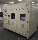
Recently, Beijing Hualin Jiaye Technology Co., Ltd. (CGB) successfully delivered a self-developed wet cleaning equipment cluster to a leading domestic third-generation semiconductor company. This important milestone marks that my country has made substantial breakthroughs in the field of key equipment for silicon carbide (SiC)/gallium nitride (GaN) wafer manufacturing, providing strong support for the independent control of the industrial chain. The equipment will be used in silicon carbide epitaxy and device production lines to help improve wafer manufacturing yield and production efficiency. Especially in the field of silicon carbide power devices, its excellent high-voltage and high-temperature resistance make it a core device for high-end applications such as electric vehicles and photovoltaic inverters.

The delivered equipment constitutes a complete cleaning chain: from the development/stripping of the photolithography link (semi-automatic development machine, inorganic stripping cleaning machine), to post-etching processing (dielectric/silicic acid-alkali etching station), to the ultimate cleaning (multiple types of ultrasonic cleaning machines), and even special material processing (silicon carbide wafer cleaning machine), forming a closed loop of 8 key process nodes.

As a leading professional semiconductor equipment manufacturer in China, CGB focuses on the R&D and production of wafer cleaning, drying and surface treatment technologies. The company's R&D headquarters is located in Beijing Yizhuang Economic and Technological Development Zone, with a northern production base in Langfang, Hebei and a Wuxi East China regional service center. It also has a R&D center in Japan, focusing on product development and overseas market services.

Product application areas include: integrated circuits (IC), micro-electromechanical systems (MEMS), silicon materials (Si), compound semiconductors (Compound Semiconductor), optical communication devices (Optical Communication Devices), power devices (Power Devices), semiconductor lighting (LED), advanced packaging (Advanced Packaging), photovoltaic cells (Photovoltaic), flat panel displays (FPD) and scientific research (R&D), etc.​

1752771190302.png1752771205300.png
1752771236318.png

Please, Log in or Register to view URLs content!
 

tokenanalyst

Brigadier
Registered Member

Tuojing Technology expects revenue of 1.21 billion to 1.26 billion yuan in Q2, and net profit is expected to increase by 101% to 108% year-on-year​


On July 17, Tuojing Technology Co., Ltd. (stock code: 688072, hereinafter referred to as "Tuojing Technology") released its second quarter 2025 performance forecast, and it is expected that the company's operating income, net profit and net cash flow from operating activities will all achieve significant growth.

According to the announcement, Tuojing Technology expects to achieve operating income of RMB 121 million to RMB 126 million in the second quarter of 2025, a year-on-year increase of 52% to 58%. Net profit attributable to the parent company's owners is expected to be RMB 238 million to RMB 247 million, a year-on-year increase of 101% to 108%. Net profit after deducting non-recurring gains and losses is expected to be RMB 215 million to RMB 224 million, a year-on-year increase of 235% to 249%. In addition, the company expects net cash flow from operating activities in the second quarter of 2025 to be RMB 148 million to RMB 158 million.

Compared with the second quarter of 2024, Tuojing Technology's performance has improved significantly. In the same period of 2024, the company achieved operating income of 795.101 million yuan, net profit attributable to the parent company's owners was 118.6223 million yuan, net profit after deducting non-recurring gains and losses was 64.1667 million yuan, and net cash flow from operating activities was -178.4617 million yuan.

Tuojing Technology also stated that the main reasons for the performance growth in the second quarter of 2025 include:​
  1. Increased market penetration : The company actively seizes the strategic opportunity of domestic substitution of semiconductor equipment, relying on the technological leadership of thin film deposition equipment (PECVD/ALD/SACVD/HDPCVD/Flowable CVD) and advanced bonding equipment in the field of three-dimensional integration and supporting quantity detection equipment. The product maturity and performance advantages have been widely recognized by customers, the market penetration rate has been further improved, and the revenue has continued to grow rapidly.​
  2. New product mass production breakthrough : The company's advanced process verification equipment has successfully passed customer certification and gradually entered the large-scale mass production stage. Advanced process equipment such as PECVD Stack (ONO stacking), ACHM and PECVD Bianca based on new equipment platforms (PF-300T Plus and PF-300M) and new reaction chambers (pX and Supra-D) have successively passed customer acceptance, and the scale of mass production has continued to increase; ALD equipment continues to expand its mass production scale, with strong business growth, and sales revenue in the second quarter of 2025 will exceed the annual revenue scale of 2024.​
  3. Improved gross profit margin : The new product verification machine has completed technology introduction and achieved breakthroughs in mass production and continuous optimization. The gross profit margin in the second quarter of 2025 improved significantly month-on-month, showing a steady recovery trend.​
  4. Decrease in expense ratio : The expense ratio during the period decreased year-on-year, and the scale effect further released profit space.​
  5. Increased cash flow from operating activities : In the second quarter of 2025, the company's prepayments and sales proceeds both increased significantly compared with the same period last year, and the net cash flow generated from operating activities increased significantly compared with the same period last year.​

Please, Log in or Register to view URLs content!
 

tokenanalyst

Brigadier
Registered Member

Shanghai Municipal Science and Technology Commission 2025 Research Program "Integrated Circuit" project (some of the projects):​


Research on plasma extreme ultraviolet light sources driven by high-current electron beams

Goal: To meet the needs of high-power EUV lithography, we will study plasma EUV light sources driven by medium-energy (<10MeV) high-current electron beams. We will conduct theoretical modeling and high-precision simulation of the entire process of generating high-temperature plasma and EUV radiation driven by high-repetition-rate (~100MHz) electron beams, optimize the key parameters of electron beams and plasma, and generate EUV radiation power >100W at the target IF point.

High-precision spectrum research of lithography light sources

Objectives: To conduct high-precision research on the spectral lines of 17- and 18-valent gadolinium (Gd) ions, experimentally obtain high-precision spectral lines in the 5.7-7.7nm band, and the wavelength uncertainty of the spectral lines near the 6.Xnm band is less than 0.004nm.

Based on electron beam ion trap, high-precision flat-focus field spectrometer and other devices, carry out experimental research on 17 and 18 valence Gd high-charge state ion spectra. Use the internal calibration method to eliminate the systematic deviation caused by the difference in ion position and achieve high-precision measurement of the spectrum. At the same time, combined with the atomic structure calculation package, simulate and analyze the spectral lines of Gd ions with different valence states, providing key experimental and theoretical data support for the optimization research of lithography light sources.

Research on high-power laser-driven X-ray light sources

Goal: To meet the needs of high-resolution X-ray lithography, explore and propose feasible solutions for the generation of efficient X-ray light sources driven by high-power lasers, with a light source energy range of 0.5-2keV and a conversion efficiency of ≥8%.


Research on synergistic defect repair at block copolymer interfaces

Objectives: To establish the collaborative design criteria for short-wavelength UV exposure pattern-block copolymer material interface, to construct a matching system between short-wavelength UV lithography pre-pattern CD size and different block copolymers and molecular weights, to enhance pattern fidelity, improve pattern roughness and local line width uniformity, and to achieve a dislocation and bridging defect density of less than 10 particles/cm2.


Dynamic in situ characterization of block copolymer polymer self-assembly.

Objectives: Study the dynamic process of block copolymer self-assembly, clarify the dynamic evolution law of 10-nanometer ordered structure, establish cross-scale (molecular-mesoscopic-macroscopic) time-space resolution characterization methodology, construct a theoretical model of self-assembly dynamics under multi-field coupling conditions, reveal the molecular mechanism of defect formation and annihilation, and form a dynamic control theoretical framework. At least two defect elimination methods should be clarified to effectively expand the film thickness process window by more than two times.


Research on the preparation of ultra-thin self-supporting spectral purification films

Goal: To meet the needs of next-generation lithography spectrum purification, break through the key technologies of ultra-thin self-supporting films, develop high-strength large-area film preparation methods, and achieve 6.Xnm transmittance > 70%, film thickness < 200nm, and film diameter > 20mm.


Design and synthesis of new photoacid-bonded monomers and their application in extreme ultraviolet lithography

Research objective: To address the randomness issues caused by low photon absorption rate and easy diffusion of protons in extreme ultraviolet photoresists, explore the synthesis of novel photoacid-bonded monomers (purity ≥98%, metal impurities ≤20ppb, storage stability ≥6 months) and resins containing them (photoacid-bonded copolymer resin molecular weight ≤8000, molecular weight deviation between reaction batches ≤500, molecular weight distribution ≤1.4, and the molar ratio/sequence of each copolymer monomer in the resin is stable and controllable) to achieve lithography resolution ≤18nm and line edge roughness ≤2nm.

Research on two-dimensional semiconductor atomic layer etching

Objectives: Develop controllable atomic layer etching processes with atomic-level precision for sub-nanometer node advanced structure two-dimensional semiconductor devices. Develop ≥3 types of ALE processes with atomic-level precision for semiconductors such as MoS2, WS2, and WSe2, achieve angstrom-level uniformity (RMS roughness ≤ 0.1nm) and atomic layer etching accuracy ≤ 0.7nm/cycle on 4-inch wafers; establish a theoretical model of atomic-level reactions of two-dimensional semiconductors, and reveal ≥3 related ALE reaction mechanisms.

Research on intelligent large-scale models of advanced lithography equipment

Objectives: Develop a dynamic digital twin of the ultra-precision electromechanical system of advanced lithography equipment driven by theory-data fusion, and achieve microsecond-level dynamic simulation and greater than 95% simulation consistency. Construct an intelligent large model of the ultra-precision electromechanical system of advanced lithography equipment, and achieve an improvement of more than 10% in parameter prediction accuracy and more than 90% in fault prediction accuracy. Support intelligent optimization and precise decision-making in the debugging and operation of the ultra-precision electromechanical system of advanced lithography equipment, and improve system reliability and operation efficiency.

Research on prediction of extreme ultraviolet high-resolution photoresist performance based on small data sets

Goal: To solve the problem of predicting the performance of extreme ultraviolet high-resolution photoresists, based on the chemical information and process parameters of photoresists, develop an interpretable and transferable theory-driven machine learning model to predict photoresist process characteristics and lithography performance indicators (resolution, sensitivity, roughness, and key dimension consistency). It is required to predict ≥5 key process characteristics and lithography performance prediction error ≤5%; the amount of data required for migration training is ≤100, and the lithography performance prediction error is ≤10%.

-
Most are expected to be completed in the next 2 years.
 
Top