Chinese semiconductor thread II

Schmoe

New Member
Registered Member
"The latest results of the pilot line of domestic immersion deep ultraviolet lithography machine: short-stroke positioning accuracy is 2nm, medium-stroke positioning accuracy is 3nm, and long-stroke positioning accuracy is 5nm"

Can anybody comment on how that translates to node size for HVM? What positioning accuracy does the 1980Di have? I could not find anything via quick Google searches deciphering the implications of this.
 

tokenanalyst

Brigadier
Registered Member
"The latest results of the pilot line of domestic immersion deep ultraviolet lithography machine: short-stroke positioning accuracy is 2nm, medium-stroke positioning accuracy is 3nm, and long-stroke positioning accuracy is 5nm"

Can anybody comment on how that translates to node size for HVM? What positioning accuracy does the 1980Di have? I could not find anything via quick Google searches deciphering the implications of this.

Stroke position accuracy I think is referring to the accuracy of the Maglev Motors or the motion system. Overlay is distinct.
 

interestedseal

Junior Member
Registered Member
This has already been posted, and it's not an EUV lithography machine or part of one, but an interferometer for calibrating EUV optics. AKA it's part of the tooling for manufacturing EUV machines and a good indicator that China is at very least close to a finished product, but it's not the product itself
At least three such interferometers in this image if you look carefully. Are they preparing for mass production?
 

measuredingabens

Junior Member
Registered Member
I've seen some hubbub in the last few months of Huawei working on LDP (developed by Harbin Institute of Technology), as opposed to LPP EUV lithography machines. How credible are these rumours? CIOMP's project seemed to be nearest to completion (or even completed), judging from the patents.
 

OptimusLion

Junior Member
Registered Member
Peking University team establishes new Big-MEMS thermal measurement method

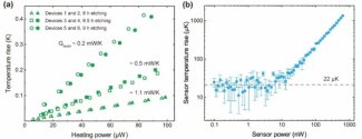
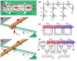
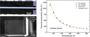
The team led by researcher Song Bo from Peking University proposed the new concept of Big-MEMS thermal measurement in early 2023. The core of the Big-MEMS concept is to design and manufacture thermal measurement devices suitable for macro-scale samples based on standard MEMS processes, thereby fundamentally expanding thermal measurement capabilities. As a demonstration, the research team developed a novel process flow that can reliably, reconfigurably, modularly and cost-effectively manufacture silicon-based suspended heating/calorimetric devices with sizes ranging from millimeters to centimeters.

94aef9b2b3b0a0fd7aa8da40d404dbcf (1).jpg

539538ccc411d84052d9b1e1b373df43 (1) (1).jpg

92fa21cc7d639ce2120511994246e8f9 (1) (1).jpg

7a83df23512b545160bf1ba44cfe8ae4 (3).jpg

f8c82aed7c69acefc7850e6bc528af4d (1).jpg
Please, Log in or Register to view URLs content!
 
Last edited:

Hyper

Junior Member
Registered Member
I've seen some hubbub in the last few months of Huawei working on LDP (developed by Harbin Institute of Technology), as opposed to LPP EUV lithography machines. How credible are these rumours? CIOMP's project seemed to be nearest to completion (or even completed), judging from the patents.
LDP is for mask defect detection. Ushio has a similar tool.
 

OptimusLion

Junior Member
Registered Member
National People's Congress Representative, HGTECH Ma Xinqiang: China's laser industry has entered the world's first echelon

On March 8, during the second "Representative Channel" interview activity of the Third Session of the 14th National People's Congress, National People's Congress Representative, Huagong Technology Party Secretary and Chairman Ma Xinqiang was interviewed and introduced how China's laser equipment field has cracked the "bottleneck" technology and achieved scientific and technological self-reliance. "Today we can confidently say that China's laser industry has entered the world's first echelon." Ma Xinqiang said, "But innovation is a long-distance race with no end. We will continue to work hard and take difficult roads to reshape new advantages for the optoelectronics information industry and strive to be the vanguard of innovation in the high-end equipment industry."

600aeab24c52af8af95e7bc28060c244 (1).jpg

Please, Log in or Register to view URLs content!
 

tokenanalyst

Brigadier
Registered Member
Kudos to the US government, they have achieved in less than five years what the Chinese government couldn't in three decades.
Especial thanks to Alan Estevez, Gina Raimondo, the overpaid think tankers stooges at CSIS and CSET. Without their puddle shallow understanding of 5G, AI and the semiconductor industry, this feat would have been very difficult.


1741536315589.png
 
Top