Chinese semiconductor thread II

tphuang

General
Staff member
Super Moderator
VIP Professional
Registered Member
Please, Log in or Register to view URLs content!

Nexchip result here, very interesting on the 28nm process
今年上半年,
Please, Log in or Register to view URLs content!
预计CIS占主营业务收入的比例将持续提高。在DDIC继续巩固优势的基础上,CIS成为该公司第二大主轴产品,其他产品竞争力稳步提升。
工艺节点方面,目前
Please, Log in or Register to view URLs content!
40nm高压OLED显示驱动芯片已实现批量生产,55nm全流程堆栈式CIS芯片实现批量生产,28nm OLED显示驱动芯片及28nm逻辑芯片研发进展顺利,预计今年年底可进入风险量产阶段
55nm CIS has entered mass production and so has 40nm OLED DDIC. They are entering risk production for 28nm OLED DDIC and 28nm logic chip by end of this year.
 

tokenanalyst

Brigadier
Registered Member

whether 5nm process is happening and at what yield is not known, but the original poster is not a reliable source. Even if he happens to be right here, he still has been wrong plenty of times before. That is my point. If they do start fabbing "5nm process", we still will need some time to get info on the critical features/dimensions and such. Again, this poster has not been a reliable source for that either.
We would have to wait for the techinsights decapping and SEM study.
 

tokenanalyst

Brigadier
Registered Member

Shengmei Shanghai and East China University of Science and Technology jointly build a joint technology innovation and transfer center for high-end semiconductor equipment.​


East China University of Science and Technology and ACM Semiconductor Equipment (Shanghai) Co., Ltd. (hereinafter referred to as "ACM Shanghai") officially signed an agreement to jointly build the "East China University of Science and Technology-ACM Shanghai High-end Semiconductor Equipment Joint Technology Innovation and Transfer Center". This signing marks the start of all-round and in-depth cooperation between the two parties in terms of technological breakthroughs, achievement transformation and talent training.

Shengmei Shanghai has always focused on product quality, technical level and customer service, continuously improving the content of existing equipment and deepening the expansion and research and development of existing product lines. It has successfully laid out seven major product segments, including cleaning equipment, electroplating equipment, advanced packaging wet process equipment, vertical furnace equipment, glue coating and development equipment, PECVD equipment and panel-level packaging equipment. The essence of chip manufacturing is precision chemical reaction. East China University of Science and Technology has a profound academic accumulation in the fields of chemical reaction analysis, and the cooperation between the two parties is highly compatible. In the past three years, East China University of Science and Technology has sent more than 30 outstanding graduates to Shengmei Shanghai, and many masters and doctors have become the backbone of the company's R&D.

Jia Shena, vice president of Shengmei Shanghai, said that in the future, the cooperation between the two sides will focus on tackling scientific problems in wet process technology and exploring new paths for the integration of industry, academia and research; deepen talent training, and cultivate high-end, compound talents through mechanisms such as joint training of engineering masters and doctoral students and dual-appointment of tutors by schools and enterprises.

The joint laboratory established by Shengmei Shanghai and East China University of Science and Technology is a recognition of previous cooperation and an expectation for the future. We believe that driven by both scientific and technological research and talent training, the joint laboratory will produce more innovative results and contribute more "Chinese solutions" to the global semiconductor industry.

Please, Log in or Register to view URLs content!
 

sunnymaxi

Major
Registered Member
NAND and memory is a good start for high end SAQP Lithography, its require high density but the structures are simple enough that allow for a better finetune of the lithography process than logic.
YMTC is actually in a solid position.. they are one of the earliest victims of American chip war. have been blacklisted since 2022. they immediately shifted on domestic firms and started to work with NAURA/AMEC plus their own R&D like Hybrid bonding tech helping them to leapfrog the market leaders.

now this latest news is about 100 percent domestic supply chain include Litho scanner.. we knew it, this was coming.

CXMT is also on the same path.
 
Last edited:

tokenanalyst

Brigadier
Registered Member

MPCVD diamond material and high-end wafer project officially started.​


Liaoning Shenfu Reform and Innovation Demonstration Zone ushered in important progress in the integrated circuit industry. The "Fourth Generation Semiconductor MPCVD Diamond Materials and High-end Wafer Production Base" jointly invested by Hydrogen New Energy Technology Group and the main investor Shanghai Zhuoyuan Fangde Semiconductor Co., Ltd. officially broke ground.

The total investment of the project is about 3 billion yuan, with a planned land area of 165 mu, and it is committed to building a world-class intelligent green semiconductor material production base. The core of the project focuses on the cutting-edge fourth-generation semiconductor material - MPCVD diamond , which has excellent properties such as ultra-wide bandgap, high thermal conductivity, and high breakdown field strength, and is a key material to break through the bottleneck of extreme application scenarios.

The project will introduce advanced MPCVD diamond material production lines and 12-inch electronic-grade large wafer material production lines and other high-end intelligent manufacturing equipment, deeply integrating intelligent production and intelligent management. After the project is fully completed, it is expected to form an annual production capacity of 4.8 million high-end wafers.

The commencement of construction marks that the development of the project in the Shenfu Demonstration Zone has entered the fast lane. Back to March 17 this year, the project has held a groundbreaking ceremony in the name of "Shanghai Zhuoyuan 12-inch wafer production base" and has received great attention from the local government. Zhang Xinfeng, chairman of Shanghai Zhuoyuan Fangde Semiconductor Co., Ltd., said at the groundbreaking ceremony: "The Shenfu Demonstration Zone has a good ecological environment, superior location and transportation, and complete industrial supporting facilities. It has the best service and policy environment and is a real investment hot spot."​

Please, Log in or Register to view URLs content!
 

tokenanalyst

Brigadier
Registered Member

Xinde Semiconductor received nearly 400 million in financing, catalyzing the breakthrough of domestic chiplets​


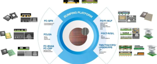
Recently, Jiangsu Xinde Semiconductor Technology Co., Ltd. has officially completed a new round of financing, which was jointly led by the city/district institutions, and followed by Yuanhe Puhua, Provincial New War Fund, and Yushan Capital. The amount of this round of financing reached nearly 400 million yuan, which will be mainly used to further accelerate the layout of SiP (system-level packaging), FOWLP (fan-out wafer-level packaging), Chiplet-2.5D/3D, heterogeneous packaging modules and other high-end packaging and testing technology research and development and production .

Jiangsu Xinde Semiconductor Technology Co., Ltd. was established in September 2020. It is an integrated circuit company that grew up in Nanjing and is dedicated to mid-to-high-end packaging and testing. Currently, it can provide customers with Bumping, WLCSP, Flip Chip PKG, QFN, BGA, SIP, SIP-LGA, and 2.5D packaging product design and services.

1753121633397.png
  • Optical communication field: The 2.5D/3D structure products created by the Xinde Semiconductor R&D team use 5nm process top die wafer technology, which has reached the top level in the industry and has been shipped. Currently, a cooperation intention has been reached with a leading domestic GPU design company.​
  • TGV: This packaging technology is becoming a core solution in the field of advanced packaging due to its ultra-high frequency performance, low-loss interconnection and excellent thermal stability. After nearly a year of concentrated research and development, Xinde Semiconductor has made significant progress in this technology and is expected to complete sample production in collaboration with Southeast University by the end of July 2025.​
  • TMV: Through the plastic package through-hole technology, vertical high copper pillars are processed in the plastic package, and the copper pillars connect the RDL redistribution layers on both sides, thereby reducing signal delays and improving signal transmission speed and integrity. In order to overcome this technology, the company has undergone years of continuous research and development, from process solution design to repeated test optimization, and continuously breaking through technical difficulties. At present, the technology has achieved phased results, and it is expected to complete sample production in July, and reach a cooperation intention with a domestic leading artificial intelligence design company.​
  • 2D/3D light sensing products: 2D/3D light sensing products with ambient light sensing function have completed engineering batch verification, met customer requirements, and are being smoothly introduced into mass production; a number of ToF series optical packaging products have entered the feasibility assessment and investment plan discussion stage, and professional equipment will be introduced to expand the production line in the future.​
  • LPDDR: The project adopts a multi-chip stacking structure and ECF and TFV processes to achieve thinner packaging thickness, high integration and fast transmission speed. The first generation of samples has been prepared in the factory, and the second generation of samples has been more than half developed and is expected to be completed by the end of July, reaching in-depth cooperation with customers.

Please, Log in or Register to view URLs content!
 

sunnymaxi

Major
Registered Member
TGV100 Nano Air Float Motion Platform from Zhongyan Evonik: Breaking the Monopoly and Creating a New Domestic Benchmark in the Field of Semiconductor Packaging

In the journey of China's semiconductor industry striving to break through technical barriers, an exciting news came: the first large-format TGV100 nano-air flotation motion platform independently developed by Zhongyan Yingchuang Intelligent Technology Co., Ltd. was successfully launched and delivered. This milestone achievement not only marks a major leap forward in the field of high-end semiconductor packaging core equipment, but also injects a strong localization impetus into the development of China's advanced packaging technology, allowing the world to see China's hard-core strength in the field of semiconductor precision manufacturing.

153619_212660_newsimg_news.png


Please, Log in or Register to view URLs content!
 
Top