Chinese semiconductor thread II

tokenanalyst

Lieutenant General
Registered Member

Huahai Qingke Establishes Shanghai Headquarters in Jinqiao Equipment Town to Advance Semiconductor Equipment Manufacturing


Huahai Qingke (Shanghai) Semiconductor Co., Ltd. has signed an agreement to establish a comprehensive Shanghai headquarters within Jinqiao Equipment Town Innovation Park. The facility will focus on high-end integrated circuit (IC) equipment for advanced manufacturing processes and packaging, including ion implantation, chemical mechanical polishing (CMP), and high-precision grinding equipment.

The project will integrate R&D, production, sales, procurement, and services to support Shanghai’s IC industry strategy. Initial phases include:​
  • A R&D and production center targeting smaller process nodes and emerging applications (e.g., 3D IC packaging), aligning with key customers in Shanghai and the Yangtze River Delta.​
  • A customer technical service center and inventory management hub to enhance regional support, maintenance efficiency, and rapid response for advanced production lines.​
Jinqiao Equipment Town is a strategic platform for Pudong’s high-end, intelligent, and green manufacturing development. Huahai Qingke, already a semiconductor industry leader with breakthroughs in ion implantation equipment (adopted by major domestic chipmakers), aims to strengthen its "equipment + service" platform through this expansion, driving innovation in China’s semiconductor supply chain.

Please, Log in or Register to view URLs content!
 

tokenanalyst

Lieutenant General
Registered Member

Bennett Optics completes tens of millions of yuan in Series A++ financing, focusing on the LCoS chip track.​

Recently, Bennett Optics Technology (Suzhou) Co., Ltd. (hereinafter referred to as Bennett Optics) announced the completion of tens of millions of yuan in Series A++ financing. This round was exclusively invested by Anxin Investment, a professional institution in the field of semiconductor hard technology. The funds will be mainly used for core technology R&D upgrades, industrial capacity expansion, and high-end talent reserves, further strengthening its core competitiveness in the field of LCoS (liquid crystal on silicon) device localization.

1765902226053.png
1765902324625.png

Bennett Optics stated that following this round of financing, the company will focus on investing in the research and development of high-precision LCoS chips, achieving key technological breakthroughs, and improving product resolution and stability. Simultaneously, it will advance capacity expansion projects and optimize mass production process efficiency. Furthermore, it plans to leverage the advantages of the Yangtze River Delta semiconductor industry cluster to deepen its strategic layout, replicating mature technological solutions and service models to more application scenarios.

Bennett Optics is a company specializing in the R&D and industrialization of LCoS optical devices. With "innovation empowering the optoelectronic industry" as its core positioning, its business covers LCoS chip, optical device manufacturing and full-chain solution output. In particular, it has accumulated rich technical experience in sub-fields such as industrial-grade LCoS-SLM products, optical communication wavelength selective switches (WSS), precision laser processing, and projection optical engines. It has solved the pain points of technology fragmentation and high industrialization difficulty in the traditional LCoS industry. At present, its core products have achieved mass supply and have been recognized by leading companies in the industry.

Please, Log in or Register to view URLs content!
 

tokenanalyst

Lieutenant General
Registered Member

The Institute of Microelectronics has made significant progress in pulse in-memory computing architecture.​

Spiking neural networks (SNNs) are event-driven and low-power, making them ideal for deployment in edge computing scenarios such as autonomous driving and mobile healthcare. However, in real-world applications, pre-trained SNN models often struggle to directly adapt to personalized tasks due to scenario-specific biases in user data. While on-device training is considered a viable solution, achieving efficient and low-power training on resource-constrained edge hardware remains a significant challenge.

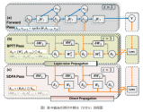
To address the aforementioned challenges, a research team from the National Key Laboratory of Integrated Circuit Manufacturing Technology at the Institute of Microelectronics, Chinese Academy of Sciences, achieved high-efficiency training of edge-end spiking neural networks in mini-batch learning scenarios through algorithm and hardware co-design. The team proposed a hardware-friendly training algorithm—Spiking Direct Feedback Alignment (SDFA)—which constructs a direct feedback path during error backpropagation. The feedback weights utilize a fully random matrix and remain fixed during training, requiring no updates and significantly reducing computational and storage overhead. At the hardware level, the team designed an efficient memristor in-memory computing architecture called PipeSDFA, fully leveraging the algorithmic characteristics of SDFA to achieve three-stage pipelined parallel processing of time steps, data, and batch processing. This architecture also utilizes the intrinsic randomness of memristor devices to efficiently store the fixed random feedback matrix. To further improve computational efficiency, the team introduced an input data reuse mechanism and proposed an efficient weight mapping scheme (vw-SDK), effectively optimizing the utilization of computational resources. Experimental results show that the SDFA algorithm maintains comparable model accuracy to baseline methods on multiple datasets, with a loss of no more than 2%. In terms of hardware performance, the PipeSDFA architecture offers a 1.1 to 10.5 times faster computation speed and a 1.37 to 2.1 times better energy efficiency compared to existing RRAM-CIM architectures (such as PipeLayer). This research effectively addresses the hardware efficiency bottleneck in edge device training and provides a scalable solution for the practical application of neuromorphic computing systems in resource-constrained environments.
1765920628884.png
The findings of this research, titled "When Pipelined In-Memory Accelerators Meet Spiking Direct Feedback Alignment: A Co-Design for Neuromorphic Edge Computing," were presented orally at the 44th International Conference on Computer-Aided Design (ICCAD) in Munich, Germany. Ren Haoxiong, a master's student at the Institute of Microelectronics, is the first author, and Shang Dashan, a researcher at the Institute of Microelectronics, is the corresponding author. This work was supported by the National Key Research and Development Program of China, the National Natural Science Foundation of China, and the Chinese Academy of Sciences.

Please, Log in or Register to view URLs content!
 

tokenanalyst

Lieutenant General
Registered Member

The Institute of Microelectronics has made new progress in the field of high-performance clock chips.​

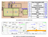
The iterative evolution of 5.5G/6G wireless communication technologies and the breakthrough of next-generation SerDes interfaces to higher transmission rates have placed more stringent demands on the jitter performance of millimeter-wave local oscillator clocks. Subsampling phase-locked loops (PLLs), with their inherent advantage of high phase detection gain, have become the mainstream solution for low-jitter clock chips. However, the charge-sharing effect in traditional subsampling phase detectors severely degrades the loop phase margin, requiring a significant increase in the master-slave sampling capacitor ratio, leading to increased power consumption in the isolation buffer. Simultaneously, to suppress the impact of binary frequency shift keying (BFS) on reference spurious signals, traditional structures require the introduction of additional dummy sampling paths, further increasing power consumption. Furthermore, in the millimeter-wave band, the lower quality factors of capacitors and varactors cause deterioration in oscillator phase noise, affecting the overall jitter performance of the PLL.

1765920718272.png

To address the aforementioned key issues, the team led by Yang Zunsong and Huang Yunbo at the Key Laboratory of Radiation-Hardened Devices Technology, Institute of Microelectronics, in collaboration with Tsinghua University, proposed a dual-edge ping-pong subsampling phase-locked loop (PLL) architecture. This architecture utilizes both the rising and falling edges of the reference clock to achieve equivalent frequency multiplication of the reference frequency, effectively solving the design trade-offs between loop bandwidth, in-band phase noise, and reference spurious emissions inherent in traditional subsampling PLLs. The team also proposed a high-power and area-efficient injection-locked buffer scheme. This structure efficiently extracts the oscillator's second harmonic while simultaneously achieving harmonic shaping, significantly reducing the out-of-band phase noise of the PLL. Based on these two technologies, the team designed and implemented a K-band PLL clock chip using a 65nm CMOS process, with an output frequency covering 22.4–25.6 GHz, overall power consumption below 18 mW, RMS integral jitter better than 50 fs, and a jitter-power figure of merit (FoM) below −254 dB.

Please, Log in or Register to view URLs content!


tokenanalyst

Lieutenant General
Registered Member

Peking University has developed an ultrasonic flow meter based on a PMUT array to achieve high frame rate flow measurement.​


From cutting-edge technologies like aerospace control and semiconductor manufacturing to common applications like household gas meters, flow meters are closely related to people's production and daily lives in many fields.

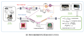
Peking University has developed an innovative ultrasonic flow meter using a piezoelectric micromechanical ultrasonic transducer (PMUT) phased array, enabling high-frame-rate, non-invasive flow measurement. Unlike traditional time-of-flight (ToF) systems that require separate transmit and receive pairs with slow, two-step processing, this new design uses a five-channel PZT PMUT array to generate symmetrical bidirectional V-shaped acoustic beams. This allows for simultaneous upstream and downstream signal detection enabling one-step flow calculations without the need for transceiver switches or complex signal processing.

The system overcomes longstanding technical limitations by eliminating the traditional λ/2 spacing constraint that causes grating lobes, while offering greater design flexibility. It employs directional transmit transducers with V-shaped beams and omnidirectional receive transducers, allowing independent optimization of transmission and reception performance. This supports planar mounting and simplifies integration into diverse industrial environments, making it more adaptable than conventional flow meters.

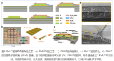
Technically, the PMUT is a compact 3.6 mm × 3.6 mm device fabricated on an SOI substrate with a layered structure including PZT film, platinum electrodes, interconnects, and protective layers. Advanced processes such as deep reactive ion etching (DRIE) and trench isolation are used to reduce mechanical and acoustic crosstalk between channels. Each of the five adjacent channels contains three PMUT units, forming an efficient phased array that delivers strong signal fidelity under real-world conditions.

This breakthrough enhances the accuracy, speed, and practicality of ultrasonic flow sensing making it ideal for applications ranging from industrial process control to household gas meters and aerospace systems. By offering a simpler, faster, and more scalable solution than existing technologies, Peking University’s PMUT-based flow meter represents a significant advancement in non-invasive fluid monitoring with broad potential across sectors requiring precise and reliable flow measurement.

1765933068742.png1765933096767.png

Please, Log in or Register to view URLs content!
 

tokenanalyst

Lieutenant General
Registered Member

XinSino completes A+ round financing of over 500 million yuan​


Recently, Suzhou Xinshinuo Semiconductor Equipment Co., Ltd., a provider of integrated solutions for domestically developed automated material handling systems (AMHS) for semiconductors, announced the completion of its Series A+ financing round, raising over RMB 500 million.

This round of financing was jointly led by Guoke Investment and China Internet Investment Fund (China Internet Investment), with participation from local state-owned asset platforms such as Wuxi Guolian, Hefei Construction Investment, and Xuhui Capital, as well as bank-affiliated investors such as Bank of China, ICBC, and Industrial Bank. Existing shareholder Hongshi Capital continued to invest.

According to available information, Suzhou Xinshinuo Semiconductor Equipment Co., Ltd.'s main business revolves around AMHS solutions for multiple fields. Its core products are represented by overhead crane systems, specifically covering three major fields: semiconductors, panels, and new energy. In the semiconductor field, it provides full-plant logistics system solutions including OHT (overhead crane system), OHB, STK and other equipment, which are suitable for semiconductor production scenarios such as 12-inch wafers. It can achieve simultaneous scheduling of more than 1,000 overhead cranes in a single plant, and has completed application cases in FAB, silicon wafer, packaging and testing. The cumulative orders in the semiconductor field exceed 1 billion.

1765933411592.png
1765933429383.png
1765933453776.png

Please, Log in or Register to view URLs content!
 

tphuang

General
Staff member
Super Moderator
VIP Professional
Registered Member
Please, Log in or Register to view URLs content!

Novosense planting a flag since been launched on HKSE.
In the first of of 2025, Novosense delivered 310m auto chips, reaching 980m in total delivery. Expected to hit 700m in all of 2025. huge jump over 363m in all of 2024. It expects auto business to be its largest business over the next 4 to 5 years.

In first 3 quarters, it was the fastest growing analog firm in China's top 5. Growing over 70% YoY. Up until 2025, China's auto analog chip market is only 10% domestic, so a huge market to grow. Each NEV can carry 40 to 50 Novosense chip, creating value of 348 RMB.

It is looking to support SerDes, AK2 ultrasonic sensor chip, ASIL-D wheel speed sensor, 4 channel D class audio amplifier and other chips.

Well, firms like this needs to succeed if China wants to ween itself off Texas Instrument and Analog Devices.
 
Top