CEC is going to unveil a TSN network switching board tomorrow at ICCAD-Expo2025. This will use its high performance FPGA HWDSW300T . This TSN switch & edge network card will be an all in one solution including chips, power supply, industrial software. Fully domestic solution. Can be used in auto web, industrial automation and aerospace.
You are using an out of date browser. It may not display this or other websites correctly.
You should upgrade or use an alternative browser.
You should upgrade or use an alternative browser.
Chinese semiconductor thread II
- Thread starter vincent
- Start date
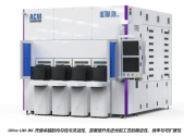
ACM Shanghai delivered its first order for the advanced photoresist curing equipment, Ultra Lith BK (Baker), which combines industry-leading UV curing and temperature control uniformity.
ACM Research (Shanghai) Co., Ltd. , a leading supplier of wafer process solutions for semiconductor front-end and advanced wafer-level packaging applications, today announced the delivery of its first order for an advanced photoresist curing equipment, Ultra Lith BK (Baker), from a leading global display manufacturer.
This equipment is specifically designed to address challenges such as insufficient uniformity, temperature drift, and critical size variation in advanced lithography processes, helping manufacturers maintain stable yields and pattern fidelity as device dimensions continue to shrink. Leveraging industry-leading UV curing uniformity and precise temperature control technology, this equipment enables highly stable and repeatable lithography processes.

Wang Jian, General Manager of Shengmei Shanghai, stated:
As lithography technology continues to push the limits of precision, maintaining uniformity in process control is crucial for achieving stable yields and device performance. The delivery of the Ultra Lith BK marks a significant milestone for ACM Shanghai – it's the first Track series device we've deployed to a client after completing initial demonstration and validation. This also signifies our formal entry into the market of display manufacturers with higher demands for equipment performance and stability, and who possess large-scale production capabilities. The Ultra Lith BK integrates high uniformity, a configurable architecture, and flexible exposure modes, helping customers significantly suppress process variations and laying the foundation for mass production expansion at future technology nodes.
Ultra Lith BK's UV curing system achieves ±5% UV intensity uniformity, ensuring uniform curing of photoresist across the entire wafer. The equipment supports line scan, rotation, and hybrid exposure modes, providing maximum process flexibility. Its advanced thermal management technology further reduces critical dimension variation, overlay errors, and pattern distortion, significantly improving yield and reliability.
Ultra Lith BK has the following features and advantages:
The Ultra Lith BK integrates six cold plates, achieving a temperature uniformity of ±0.1°C. The entire unit features a configurable design, accommodating up to 32 hot plates and two UV curing systems, allowing customers to flexibly configure it according to different process formulations and photoresist integration requirements. Hot plates are available in two sizes:
• The high-flow hot plate has a maximum process temperature of 250°C and a temperature uniformity of ≤0.2%.
• The low-flow hot plate operates at a maximum temperature of 180°C with a temperature uniformity of ≤0.08%, which is an industry-leading level.
Aiou Optics Completes Tens of Millions of Yuan in Series A+ Funding
Aiou Optics just closed a Series A+ round worth tens of millions of yuan, with investors like Daohe Tuojingxin Chain Fund and Juntong Capital. The money will go into R&D and expanding production to meet the booming demand for high-end lasers in China’s semiconductor equipment sector all to keep up with growing needs and deliver quality products on time.
Aiou Optics is a company that's blending AI with traditional optics, using an intelligent platform based on sensing, algorithms, and control. Founded in 2020 and based in Shanghai’s Zizhu Science Park, they offer advanced laser solutions like ultrafast lasers, spectral modules, and smart control systems all tailored to help the industry go smarter.
Their standout product line features "smart" lasers that can detect and analyze ultrashort pulses in real time, then automatically adjust settings for better stability and performance. This makes them super reliable for high-precision tasks like slicing wafers, cutting glass, or making display screens where consistency is key.

The company has earned top honors globally and domestically including "Global Important Advances in Optics" and the “China Laser Star Award” thanks to its deep tech expertise. They’re all about pushing optics forward with AI, following their motto: AI makes optics smart.
Their lead investor, Daohe Tuojing Chip Chain Fund, is backed by Tuojing Technology a major player in semiconductor equipment. The two already work closely together, especially on AI chip production, and are now stepping up collaboration to co-develop new tech for the future of AI chips.
Juntong Capital was involved early with a Pre-A round back in 2022, and their continued bet shows strong confidence in Aiou Optics’ long-term potential. It’s clear they see real value in the company’s innovation path.
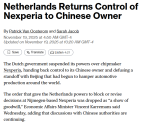
Funny way to define control when the Chinese CEO is still removed by the kangaroo court.When you put a clown in control expect an entire circus
View attachment 164911
manqiangrexue
Brigadier
Ah shit I think I spent too long in the US. I'm feeling just like Trump; the more they back down the more I wanna kick shit in their faces and call them fggts. Chinese like to give the enemy an exit so they can escape rather than push them into a battle with their backs facing the river. I want them to stand and finish the fight they started.When you put a clown in control expect an entire circus
View attachment 164911
View attachment 164912
Photolithography material manufacturer Hengkun New Materials listed on the Science and Technology Innovation Board
On November 18, Xiamen Hengkun New Material Technology Co., Ltd. (hereinafter referred to as "Hengkun New Material") was officially listed and traded on the Science and Technology Innovation Board of the Shanghai Stock Exchange.
Founded in 2004 and headquartered in Haicang District, Xiamen, Hengkun New Materials focuses on the research, development, production and sales of two key materials for integrated circuit manufacturing: photolithography materials and precursor materials. It is one of the few innovative enterprises in China with the capability to research and mass-produce key materials for 12-inch integrated circuit wafer manufacturing.
In this IPO, Hengkun New Materials plans to raise 1.007 billion yuan, primarily for the construction of the "Phase II Project of Integrated Circuit Precursors" and the "Advanced Materials for Integrated Circuits Project," helping the company further expand its production capacity, improve its technological level, and meet the ever-growing market demand. The company strives to become a leading domestic and internationally advanced local enterprise in key integrated circuit materials with core competitiveness.
Saiwei Electronics plans to acquire a portion of the equity of Xindonglai for no more than 60 million yuan.
Saiwei Electronics announced that, in order to further improve the company's industrial ecosystem layout in the semiconductor field, it plans to acquire a portion of the equity of Xindonglai for a total transaction price not exceeding RMB 60 million. The estimated valuation of Xindonglai in this transaction is no more than RMB 520 million. This transaction is expected to constitute a related-party transaction but not a major asset restructuring.
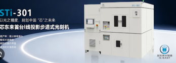
Founded in 2023, Chipdonglai is a company with mature process technology capabilities for the independent research and mass production of lithography machines. It focuses on the complete lithography machine field, with its business divided into lithography machine remanufacturing and self-developed lithography machine business. According to the announcement, the preliminary transaction plan involves Saiwei Electronics acquiring 4.11%, 3.00%, 2.80%, and 1.09% equity stakes in Chipdonglai from its original shareholders: Hainan Yimai, Intelligent Sensing Industry Fund, Xunyuan Investment, and Haichuang Intelligent Equipment, respectively.
Their first I-line projection stepper lithography machine (STi-301) has been launched, completed integration testing, and entered mass production. Fab plant verification mass production is planned for 2026.

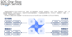
Zhancheng Technology has been awarded the title of Provincial-level "Integrated Circuit EDA Development and Design Service Innovation Center"
Recently, the Shandong Provincial Development and Reform Commission announced the "List of Provincial Service Industry Innovation Centers to be Recognized in 2025". Qingdao Zhancheng Technology Co., Ltd. (hereinafter referred to as "Zhancheng Technology"), a holding subsidiary of the company, was awarded the title of "Integrated Circuit EDA Development and Design Service Innovation Center" at the provincial level.
The integrated circuit industry is the core of the information technology industry, and a strategic, fundamental, and pioneering industry that supports economic and social development and safeguards national security. EDA, as a fundamental tool of the integrated circuit industry, plays a crucial role in improving integrated circuit design capabilities and promoting collaborative development across the industry chain.
ZC Technology's independently developed EDA software, zRC, is the first parasitic parameter extraction software in China based on FinFET technology. In 2022, it completed process adaptation for mainstream planar 28nm technology, achieving extraction accuracy and efficiency comparable to the internationally leading EDA software, StarRC. On FinFET processes, through its unique architecture design, compared to the industry-leading tool StarRC, it can improve 3D extraction efficiency by more than 50% on comparable TSMC 7nm and 14nm processes. Its technology has been certified as leading in China. Being awarded the provincial-level "Integrated Circuit EDA Development and Design Service Innovation Center" is not only a full affirmation of ZC Technology's technical strength and innovative achievements in the EDA field, but also a high recognition of the company's contributions to promoting industrial upgrading and serving industry development.


