You are using an out of date browser. It may not display this or other websites correctly.
You should upgrade or use an alternative browser.
You should upgrade or use an alternative browser.
Chinese semiconductor thread II
- Thread starter vincent
- Start date
apart from advanced Packaging ECD is very critical and important tool for High density DRAM and Flash memory chips. Lam Research, Applied Materials are the global leader in this system.
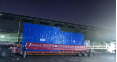
Breakthrough in the glass substrate field! Xinju Semiconductor successfully delivers its self-developed ECD equipment.

The ECD equipment delivered by Xinju Semiconductor this time represents the most challenging and critical core process equipment in glass substrate manufacturing. Notably, this equipment, along with its supporting VCL etching equipment, was entirely independently developed by Xinju Semiconductor, achieving 100% self-developed software and hardware.
The technology roadmap and application direction represent a completely new breakthrough, erasing dependence on foreign technology. In terms of technical performance, the equipment demonstrates high compatibility and stability, supporting not only 12-inch circular glass substrates but also large-size square glass substrates such as 310×310mm, 515×510mm, and 610×610mm. It can achieve stable mass production output with RDL linewidth/spacing of 2 micrometers and TGV deep via filling aspect ratio of 1:20. Its core technical indicators have reached international advanced levels, and some key performance characteristics even surpass those of similar foreign products.
Breakthrough in the glass substrate field! Xinju Semiconductor successfully delivers its self-developed ECD equipment.

The ECD equipment delivered by Xinju Semiconductor this time represents the most challenging and critical core process equipment in glass substrate manufacturing. Notably, this equipment, along with its supporting VCL etching equipment, was entirely independently developed by Xinju Semiconductor, achieving 100% self-developed software and hardware.
The technology roadmap and application direction represent a completely new breakthrough, erasing dependence on foreign technology. In terms of technical performance, the equipment demonstrates high compatibility and stability, supporting not only 12-inch circular glass substrates but also large-size square glass substrates such as 310×310mm, 515×510mm, and 610×610mm. It can achieve stable mass production output with RDL linewidth/spacing of 2 micrometers and TGV deep via filling aspect ratio of 1:20. Its core technical indicators have reached international advanced levels, and some key performance characteristics even surpass those of similar foreign products.
A breakthrough by a Shandong University team: reproducible fabrication of device-grade large-area single-crystal diamond.
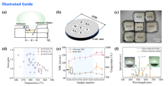
A research team led by Xu Xiangang at Shandong University has developed a novel single-crystal diamond bulk growth strategy that achieves large size, high uniformity, and excellent crystal quality—without polycrystalline edge formation (PCD rim). They identified the R value (ratio of substrate area to holder exposed area) as a key factor influencing crystal morphology and stability during thick-film chemical vapor deposition (CVD) growth. Optimal performance was found when R is between 0.6 and 0.79, ensuring stable plasma, electromagnetic field, and radical distributions, which promotes lateral expansion and suppresses edge PCD growth.

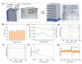
Combined with a temperature range of 880–920°C, this method enabled the growth of an 8.79 × 8.78 × 4.5 mm single-crystal diamond bulk from a small 7×7×0.5 mm substrate, maintaining a consistent triangular step-flow structure throughout. Raman and XRD analyses showed high crystal quality (FWHM ~2.0 cm⁻¹ and ~74.8 arcsec), comparable to commercial-grade materials. Crucially, cutting the bulk into seven layers retained excellent uniformity in stress, impurity levels, and crystallinity.
Device testing revealed hydrogen-terminated diamond field-effect transistors (FETs) with a maximum current density of 90–107 mA/mm, electron mobility of 76–89 cm²/V·s, and an on/off ratio of ~10⁹—showing consistent performance across all wafers.
This work presents a practical, scalable path for producing large-scale, high-quality single-crystal diamond with no edge defects, making it promising for high-power electronics, radio frequency devices, and quantum technologies. The findings advance the transition of diamond materials from lab-scale to industrial applications.

A semiconductor equipment intelligent manufacturing project with a total investment of 570 million yuan has been completed.
On November 13, the completion ceremony of the fourth phase of Zhejiang Dahe Semiconductor Industrial Park and the unveiling ceremony of FerroTec (China) Vacuum Technology Headquarters were held, marking an important upgrade of Changshan's "one chip" industrial ecosystem and laying a more solid foundation for Changshan to become an important intelligent manufacturing base for core components of global semiconductor equipment.
It is understood that the fourth phase of the industrial park project is the intelligent manufacturing project of semiconductor special equipment of Zhejiang Fulede Semiconductor Materials Co., Ltd., covering an area of 79 mu and with a total investment of 570 million yuan. It consists of three workshops: semiconductor equipment assembly workshop, surface treatment workshop and packaging machinery production workshop. It is the core carrier of FerroTec (China) Vacuum Technology Business Group.
The successful launch of this project signifies that the Daiwa Group's products will expand from the core components of semiconductor equipment (phases one, two, and three) to the assembly of semiconductor equipment components and core components for precision food packaging machinery. This will lay a more solid foundation for Changshan to become a major intelligent manufacturing base for core components of global semiconductor equipment. Once the fourth phase of the project is fully operational, it will achieve an annual production scale of over 1 billion yuan, bringing the total annual output value of the industrial park's phases one, two, three, and four to over 5 billion yuan.
"SMEE" campus recruitment for 2026
1- The poster shows two machines. The smaller one is close similar to the I-Line, KrF and dry ArF series and the big one is the interesting one.

2-They are only marketing themselves as a frontend lithography company. No packaging, no FPD, no Power Electronics. They where bought and they divested their non-frontend lithography business to AMIES

1- The poster shows two machines. The smaller one is close similar to the I-Line, KrF and dry ArF series and the big one is the interesting one.

2-They are only marketing themselves as a frontend lithography company. No packaging, no FPD, no Power Electronics. They where bought and they divested their non-frontend lithography business to AMIES

they keep hiring the new talent and people. look at the number of invention patents and National awards.. impressive"SMEE" campus recruitment for 2026
1- The poster shows two machines. The smaller one is close similar to the I-Line, KrF and dry ArF series and the big one is the interesting one.
View attachment 165006
2-They are only marketing themselves as a frontend lithography company. No packaging, no FPD, no Power Electronics. They where bought and they divested their non-frontend lithography business to AMIES
View attachment 165007
the big one in this poster also doesn't match with that 28nm Litho machine image being revealed last year.. waiting for some kind of surprise


