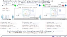
i used yandex image translate to change the text to english:Interesting roadmap about Russian lithography for 2026-2037:

You are using an out of date browser. It may not display this or other websites correctly.
You should upgrade or use an alternative browser.
You should upgrade or use an alternative browser.
Chinese semiconductor thread II
- Thread starter vincent
- Start date
Is it viable? Plus even if it suceeds(whicb is another matter altogether) does Russia doesnt have a large enough electronics market to justify such large investment/capital.Yeah the Russian plan is a 350nm solid state laser DUV lithographer (done), then KrF, ArF excimer laser DUV lithographers. This is to be followed by a Xenon plasma EUV lithographer.
They want to skip immersion lithography entirely.
Why don't we see more China/Russia coiperation in this area?
Yes is possible, they have good research institutions.Is it viable?
I think their immediate goal is to have an tool ecosystem to make ICs for the military and government projects.Plus even if it suceeds(whicb is another matter altogether) does Russia doesnt have a large enough electronics market to justify such large investment/capital.
The long term goal is to have an ecosystem of tools for making chips for their country. Given that the internal demand is not huge, they dont need huge fabs like China and TSMC do. Also, like will probably will happen in China, having a domestic ecosystem of tools will allows them to control the cost of building fabs. Maybe because the demand is not high they don't need very high throughput tools lowering the prices of these tools. The monopoly of US-Japan and ASML of semiconductor fabrication tools is one of the reasons for the huge costs.
I do think at the end both ecosystems will intertwined with both buying from each other.Why don't we see more China/Russia coiperation in this area?
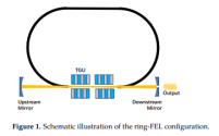
Kilowatt-Level EUV Regenerative Amplifier Free-Electron Laser Enabled by Transverse Gradient Undulator in a Storage Ring.
Abstract
High-average-power extreme ultraviolet (EUV) sources are essential for large-scale nanoscale chip manufacturing, yet commercially available laser-produced plasma sources face challenges in scaling to the kilowatt level. We propose a novel scheme that combines the high repetition rate of a diffraction-limited storage ring with a regenerative amplifier free-electron laser (RAFEL) employing a transverse gradient undulator (TGU). By introducing dispersion in the storage ring, electrons of different energies are directed into corresponding magnetic field strengths of the TGU, thereby satisfying the resonance condition under a large energy spread and increasing the FEL gain. Simulations show that at equilibrium, the average EUV power exceeds 1 kW, with an output pulse energy reaching ∼2.86 μJ, while the energy spread stabilizes at ∼0.45%. These results demonstrate the feasibility of ring-based RAFEL with TGU as a promising route toward kilowatt-level EUV sources.
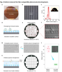
Cryo-electron tomography reconstructs polymer in liquid film for fab-compatible lithography
Abstract
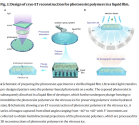
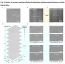
Liquid film is ubiquitous in nature and serves as the critical medium for the dissolution of photoresist to create nanoscale circuit patterns in lithography, which is a core task since the birth of semiconductor industry. However, despite decades of research, the microscopic behaviors of photoresist in liquid film and at interfaces remain elusive, leading to industrial effort for pattern defect control largely a trial-and-error process. Here, we unravel the nanostructures and dynamics of photoresist polymers in liquid film and at gas-liquid interface using a cryo-electron tomography (cryo-ET) methodology. The native-state three-dimensional structures of photoresist polymers are reconstructed by cryo-ET at significantly improved resolution compared to conventional methods. Cryo-ET reconstructions resolve the spatial distributions of photoresist polymers across gas-liquid interface into bulk solution, revealing the cohesional entanglements between polymer chains. By inhibiting the polymer entanglements and leveraging photoresist’s adsorption at gas-liquid interface, the contaminations across 12 inch wafers have been eliminated under industrial conditions, yielding a > 99% improvement in minimizing the pattern defects for fab-compatible lithography.


New generation BeiDou-3 short message communication SoC chip released
At the recently held 4th Beidou Large-Scale Application International Summit, HGI Beidou released the new generation of Beidou-3 short message communication SoC chip HD6180.
This chip integrates industry-leading technologies and indicators. Through 22nm advanced process, integrated RF transceiver SoC design, enhanced weak signal communication capability, fast signal capture capability, dual-mode decoding capability and long battery life based on ultra-low power technology, it provides industry and mass customers with a more cost-effective and competitive Beidou short message chip-level solution.
In the future, this chip will not only play a more important role in professional fields such as emergency rescue, marine fisheries, industry communications, meteorological data collection, power data collection, and logistics vehicle supervision, but will also be integrated into people's daily lives and appear more frequently in smartphones, smart watches, and smart cars.
According to the information, Beidou short message communication is a unique feature of the Beidou satellite navigation system that distinguishes it from other global satellite navigation systems. In areas without mobile communications or internet coverage, Beidou satellites provide short message communication, enabling two-way communication via satellite text messages. Beidou short message communication effectively complements terrestrial mobile communication networks, meeting the needs of emergency communications, search and rescue, and other services in areas without terrestrial network coverage. As a key component of the national emergency response system, short message communication services have played an increasingly important role in supporting people's livelihoods, disaster relief and mitigation, and field search and rescue in recent years.
Samsung Technology Leak Fuels China’s First DRAM Success
Former Samsung Electronics executives and researchers who moved to a Chinese semiconductor company and illegally used Samsung’s core national technology to develop China’s first 18-nanometer DRAM semiconductor have been indicted and detained for trial.On Oct. 1, the Information Technology Crime Investigation Department of the Seoul Central District Prosecutors’ Office (led by Chief Prosecutor Kim Yun-yong) indicted and detained three individuals, including former Samsung Electronics executive Yang, and former researchers Shin and Kwon, on charges of violating the Industrial Technology Protection Act and the Unfair Competition Prevention Act.
Yang and others are accused of moving from Samsung Electronics to CXMT (Changxin Memory Technologies), a Chinese DRAM semiconductor company, where they worked as core members of the Phase 2 Development Team. They allegedly misused Samsung Electronics’ illegally leaked 18-nanometer DRAM process core national technology to complete the development.
CXMT is China’s first DRAM semiconductor company, established with a 2.6 trillion won investment from the Chinese local government. The leaked technology is Samsung Electronics’ latest 10-nanometer class DRAM process technology, which the company developed as a world first with a 1.6 trillion won investment.
Previously, prosecutors detected signs of leakage of Samsung Electronics’ core national technology and, through direct investigation, indicted and detained two former Samsung Electronics employees: former department head Kim and former researcher Jeon, who participated in CXMT’s Phase 1 Development Team.
After further investigation into the development process, prosecutors discovered that Kim, who moved to CXMT and became the head of the Phase 1 Development Team, had illegally obtained DRAM process core national technology materials from former Samsung Electronics employee A.
Subsequently, it was found that Yang, who oversaw the entire development as the head of CXMT’s Phase 2 Development Team, Shin, who supervised process development, and Kwon, who managed practical affairs, received leaked materials from the Phase 1 Development Team. Based on these materials, they succeeded in mass-producing 18-nanometer DRAM, becoming the first in China and the fourth in the world.
The investigation revealed that they continued the work of the Phase 1 Development Team, verifying the leaked materials by reverse-engineering actual Samsung Electronics products and conducting manufacturing tests based on this information to complete the development.
It was confirmed that Shin and others received high salaries of 1.5 billion to 3 billion won from CXMT for 4-6 years, which is 3-5 times their Samsung Electronics salary, in exchange for participating in the development.
The estimated decrease in Samsung Electronics’ sales due to this incident is 5 trillion won based on last year’s figures. The future damage is expected to grow to at least tens of trillions of won.
Employee A, who is under investigation for copying hundreds of process information steps from Samsung Electronics into a notebook, is currently on Interpol’s Red Notice list.
The prosecution stated, “We will continue to respond strictly to technology leakage crimes that threaten victim companies and the national economy.”
China is doing to South Korea what South Korea did to Japan in the 80s to 2000s. Karma is a bitch. They should stop crying when they did the same thing before. Guess they now know how it feels when Japan used to complain about this same thing about them lol
Samsung Technology Leak Fuels China’s First DRAM Success
Former Samsung Electronics executives and researchers who moved to a Chinese semiconductor company and illegally used Samsung’s core national technology to develop China’s first 18-nanometer DRAM semiconductor have been indicted and detained for trial.
On Oct. 1, the Information Technology Crime Investigation Department of the Seoul Central District Prosecutors’ Office (led by Chief Prosecutor Kim Yun-yong) indicted and detained three individuals, including former Samsung Electronics executive Yang, and former researchers Shin and Kwon, on charges of violating the Industrial Technology Protection Act and the Unfair Competition Prevention Act.
Yang and others are accused of moving from Samsung Electronics to CXMT (Changxin Memory Technologies), a Chinese DRAM semiconductor company, where they worked as core members of the Phase 2 Development Team. They allegedly misused Samsung Electronics’ illegally leaked 18-nanometer DRAM process core national technology to complete the development.
CXMT is China’s first DRAM semiconductor company, established with a 2.6 trillion won investment from the Chinese local government. The leaked technology is Samsung Electronics’ latest 10-nanometer class DRAM process technology, which the company developed as a world first with a 1.6 trillion won investment.
Previously, prosecutors detected signs of leakage of Samsung Electronics’ core national technology and, through direct investigation, indicted and detained two former Samsung Electronics employees: former department head Kim and former researcher Jeon, who participated in CXMT’s Phase 1 Development Team.
After further investigation into the development process, prosecutors discovered that Kim, who moved to CXMT and became the head of the Phase 1 Development Team, had illegally obtained DRAM process core national technology materials from former Samsung Electronics employee A.
Subsequently, it was found that Yang, who oversaw the entire development as the head of CXMT’s Phase 2 Development Team, Shin, who supervised process development, and Kwon, who managed practical affairs, received leaked materials from the Phase 1 Development Team. Based on these materials, they succeeded in mass-producing 18-nanometer DRAM, becoming the first in China and the fourth in the world.
The investigation revealed that they continued the work of the Phase 1 Development Team, verifying the leaked materials by reverse-engineering actual Samsung Electronics products and conducting manufacturing tests based on this information to complete the development.
It was confirmed that Shin and others received high salaries of 1.5 billion to 3 billion won from CXMT for 4-6 years, which is 3-5 times their Samsung Electronics salary, in exchange for participating in the development.
The estimated decrease in Samsung Electronics’ sales due to this incident is 5 trillion won based on last year’s figures. The future damage is expected to grow to at least tens of trillions of won.
Employee A, who is under investigation for copying hundreds of process information steps from Samsung Electronics into a notebook, is currently on Interpol’s Red Notice list.
The prosecution stated, “We will continue to respond strictly to technology leakage crimes that threaten victim companies and the national economy.”
According to Korean Media, YMTC Jumps Straight to 400 Layers.
China’s NAND flash maker YMTC is developing a 400-layer NAND product as the next step after its current 267-layer mass-production line..
YMTC’s technological confidence comes from its pioneering use of hybrid bonding for NAND stacking. The company applied this next-generation packaging technique to mass production earlier than Samsung, SK hynix, or Micron. YMTC is now researching its fifth-generation hybrid bonding process (Xtacking 5.0) to enable over-400-layer fabrication. Industry insiders expect YMTC’s 400-layer NAND to hit the market as early as late next year.


