Yeah that's one of the few on the record announcements we have and it is a good sign but in the interim it's hard to really know where things are and we probably won't get many more announcements like that one. Further this is a roadmap, not an announcement of where the currently are. Still it is pretty encouraging but I'm going to wait until I see them come out with at least some of the stuff on that roadmap before assuming they are really on track.The closest we have to a formal announcement is Huawei's AI roadmap from a few weeks ago. Tphuang did a good analysis of it. It seems that Huawei thinks they'll have EUV by 2028 or so. And the fact that they are openly talking about it shows they are confident.
You are using an out of date browser. It may not display this or other websites correctly.
You should upgrade or use an alternative browser.
You should upgrade or use an alternative browser.
Chinese semiconductor thread II
- Thread starter vincent
- Start date
It is going to get worse for UMC. Hua Hong Wuxi Phase II will add 100k wpm 55-40nm. Nexchip and SMIC are quickly growing 40-28nm capacity.
I estimate that after Hua Hong Wuxi Phase III is done in late 2020s, which I expect will be for 28nm, just Hua Hong alone will have more chipmaking capacity than UMC.
I estimate that after Hua Hong Wuxi Phase III is done in late 2020s, which I expect will be for 28nm, just Hua Hong alone will have more chipmaking capacity than UMC.
Even though the road map isn't an official announcement, we should treat it as such because it's an official source that gives us information about the situation on the ground.Yeah that's one of the few on the record announcements we have and it is a good sign but in the interim it's hard to really know where things are and we probably won't get many more announcements like that one. Further this is a roadmap, not an announcement of where the currently are. Still it is pretty encouraging but I'm going to wait until I see them come out with at least some of the stuff on that roadmap before assuming they are really on track.
If Huawei thinks they'll get advanced nodes by 2028 and tells everyone, we should probably believe them because we don't know any better.
Applied Materials Expects $710 Million Revenue Hit From New Export Rule
Applied Materials expects a $710 million hit to its revenue from new export restrictions published by the Bureau of Industry and Security this week.
Applied Materials said Thursday the new rule would restrict its ability to export certain products to China-based customers without a license. The company said the new rules would hurt fourth-quarter revenue by $110 million and 2026 revenue by $600 million.
With a total investment of RMB 2.3 billion, Kangying Semiconductor's headquarters base was established in Quzhou, creating a valuable storage industry hub.
Recently, the foundation stone for Kangying Semiconductor's headquarters base was officially laid in Quzhou, Zhejiang Province. This milestone not only marks a new starting point for this storage-focused company to establish itself in China and establish a global presence, but will also inject strong momentum into the coordinated development of the semiconductor industry in the Yangtze River Delta, contributing to the rapid development of China's semiconductor industry.
Quzhou lays the foundation for industrial development
Since its establishment, Kangying Semiconductor has always focused on the storage field and is committed to providing ultra-reliable storage innovation solutions to global customers. Faced with multiple industry challenges, the company has always moved forward firmly: from focusing on product design and development to expanding diverse application scenarios, from continuously enriching supply chain resources to deeply linking platform manufacturers, customers and other resources, from deeply cultivating storage technology research and development to deploying national industrial bases, each step has been solid and steady. Among them, the successive production of the Xuzhou and Yangzhou industrial parks has accumulated rich experience in memory chip manufacturing for the company and also laid a solid industrial foundation for cross-regional collaboration; and the laying of the foundation stone for the Quzhou headquarters base is not only a key step in the company's capacity upgrade, but also a more intuitive reflection of this deep industrial strength that has been tested by practice, making the development foundation of the headquarters project more solid.
Kangying Semiconductor's headquarters base in Quzhou, with a total investment of 2.3 billion yuan and a total construction area of 250,000 square meters, is positioned as a "full-industry chain integrated manufacturing base," covering all functions including R&D, production, and supporting services. It will implement a full process layout from wafer grinding and cutting, high-end packaging and testing, to module product production. The project will be implemented in phases. Phase I is expected to enter trial production in Q4 2026, at which time it will establish large-scale production capacity for high-end memory chips, effectively alleviating the domestic market demand for high-end memory devices. Within 12 months of Phase I's commissioning, Phase II construction will commence, further expanding production capacity and creating a new frontier for the storage industry. This will help China's storage industry enhance its global competitiveness and achieve high-quality development, ultimately realizing the goal of "making Chinese chips a global force and domestic storage shine globally."
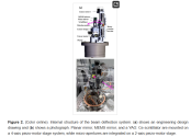
High-Precision Beam Deflection and Diagnostics System for EUV Synchrotron Radiation Illumination
Abstract
The EUV light emitted by the synchrotron radiation source exhibits a stable wavelength and pollution-free characteristics, making it highly suitable for technical verification in diverse EUV lithography applications and playing a pivotal role in EUV lithography industry research. To guide the EUV light from the beamline into the experimental platform, this paper proposes a deflection system design based on the Shanghai Synchrotron Radiation Facility (SSRF). This system enables beamline diagnostics for EUV light while facilitating precise positioning and performance testing of the Mo/Si multilayer planar deflection mirror. The deflection system achieves accurate installation and alignment through a coordinate transfer protocol. By imaging the EUV incident light spot on a scintillator and analyzing variations in EUV light intensity data before and after the deflection mirror, the system can accurately measure focused light spot parameters from the beamline and achieve submicron alignment accuracy with 10 μrad angular resolution for the deflection mirror. The proposed design provides valuable insights for advancing EUV lithography technology utilizing synchrotron radiation sources.


China's glass substrates, TGV technology breakthroughs, technological independence is expected
Dongxu Group, a leading domestic electronic glass company, has successfully completed the development of the first batch of TGV-related products and sent samples to downstream customers. Its products cover 6-inch, 8-inch, and 12-inch wafer-level specifications as well as 510×515mm board-level products, and many key technical indicators have reached world-class levels. Dongxu's breakthrough is due to its original laser-induced etching and drilling technology , combined with customized etching liquid, to achieve through-hole roundness ≥95%, aperture ≥20μm, aspect ratio 10:1, and roughness control below 1nm. In the copper plating process , they use double-sided vertical electroplating technology to achieve 100% through-hole filling, copper layer bonding strength >5N/cm, and a continuous seed layer without breakpoints, ensuring excellent electrical connection performance.
Jiangxi Vog Optoelectronics is another major player. The company boasts thick copper-on-glass technology , which it claims is "absolutely leading in the industry." Vog Optoelectronics' ultra-thin UTG-on-glass technology enables the company's glass-based circuit boards for applications in displays, communications, and advanced semiconductor packaging. Notably, Vog Optoelectronics explicitly states that its glass-based substrates are primarily used for high-computing chips , which perfectly meets the urgent demand for computing power in the AI era.
Guangdong Triassic pioneered TGV 3.0, achieving breakthroughs in sub-10-micron via and filling technology, placing it at the forefront of the international market. In 2022, the company completed a pilot line for TGV substrates and 3D integrated packaging in Songshan Lake, Dongguan. The company also participated in the establishment of a strategic scientist team for integrated circuit and semiconductor specialty processes, establishing Triassic as a leading TGV R&D and production base in mainland China with distinct characteristics and advantages.
Of particular note, OLED giant BOE , building on its existing display technology expertise, has developed a semiconductor solution featuring TGV. Its new 8-inch pilot line is now operational, featuring numerous innovative breakthroughs, including high-density 3D interconnects and high-aspect-ratio TGV technology. BOE utilizes standard glass core substrates and packaging substrates, which offer high strength and low warpage. These substrates are primarily targeted at AI chips, with mass production planned to begin after 2026.
Furthermore, a number of active companies have emerged in China's glass substrate industry chain. Xiamen Yuntian Semiconductor has shipped over 20,000 wafer-level packaging units, successfully breaking through the technical bottleneck of 4µm apertures and mastering 2.5D high-density glass interposer technology. Chengdu Yicheng Technology was among the first in China to achieve mass production of glass panel-level packaging, achieving mass production of the board-level high-density FOMCM platform, becoming the only company in mainland China currently capable of mass production of this product. Guangdong Fozhixin Microelectronics specializes in board-level fan-out packaging and glass substrate processing and manufacturing, with a minimum aperture of 1µm and an aspect ratio of 150:1. The company also operates China's first independently owned large-scale fan-out packaging mass production line.
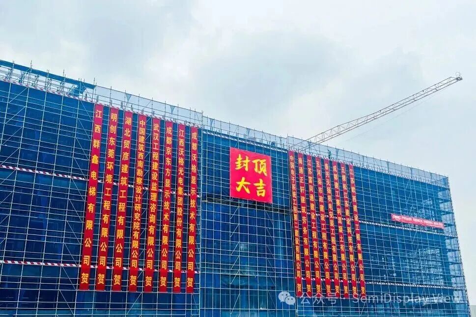
The main building of China's first 8.6-generation OLED glass-based photolithography and finishing project has been topped out
On September 30, Vog Optoelectronics announced that the main building of the world's first and China's first 8.6-generation AMOLED glass-based photolithography and finishing project, which it invested in and constructed, was topped out in Chengdu Hi-tech Zone.

The project, with a total investment of over 628 million yuan, officially began construction on April 9, 2025. It includes a main production building, auxiliary production rooms, power rooms, warehouses, and other supporting facilities, covering a total area of approximately 56 mu (approximately 1,000 square meters). The main building, which has been topped out, has three floors and a total construction area of 59,000 square meters.
After the project is completed, Chengdu Voge will become the world's first intelligent production line with the ability to mass-produce 8.6-generation AMOLED thin films, and will provide core supporting support for the mass production of 8.6-generation AMOLED lines of leading companies such as BOE.
Vog Optoelectronics said that in the next three months, the company will step up the decoration of the factory, the installation of power facilities such as water, electricity and gas, and the purchase and commissioning of production equipment to ensure that the first batch of product thinning and wafer testing will be completed in mid-January 2026, thereby achieving seamless connection with BOE's Chengdu 8.6-generation AMOLED production line mass production node.
According to information, Vog Optoelectronics specializes in the development of glass-based thinning, coating, cutting, touch display, and glass-based precision integrated circuit finishing industries. The company's core businesses include traditional displays, new displays, automotive displays, and semiconductors. Its products primarily include glass thinning, coating, precision circuit fabrication, LCD cutting, new flexible materials, automotive touch screens, high-end optical film materials, and backlight sources.

