Chinese semiconductor thread II

measuredingabens

Junior Member
Registered Member

Researchers develop world-leading microwave photonics chip for high-speed signal processing​

A research team led by Professor Wang Cheng from the Department of Electrical Engineering (EE) at City University of Hong Kong (CityUHK) has developed a world-leading microwave photonic chip that is capable of performing ultrafast analog electronic signal processing and computation using optics.

The chip, which is 1,000 times faster and consumes less energy than a traditional electronic processor, has a wide range of applications, covering 5/6G wireless communication systems, high-resolution radar systems, artificial intelligence, computer vision, and image/video processing.

The team's findings were published in Nature in a paper titled "Integrated Lithium Niobate Microwave Photonic Processing Engine." It is a collaborative research with The Chinese University of Hong Kong (CUHK).

The rapid expansion of wireless networks, the Internet of Things, and cloud-based services has placed significant demands on underlying radio frequency systems. Microwave photonics (MWP) technology, which uses optical components for microwave signal generation, transmission, and manipulation, offers effective solutions to these challenges. However, integrated MWP systems have struggled to simultaneously achieve ultrahigh-speed analog signal processing with chip-scale integration, high fidelity, and low power.

"To address these challenges, our team developed a MWP system that combines ultrafast electro-optic (EO) conversion with low-loss, multifunctional signal processing on a single integrated chip, which has not been achieved before," explained Professor Wang.

Such performance is enabled by an integrated MWP processing engine based on a thin-film lithium niobate (LN) platform capable of performing multi-purpose processing and computation tasks of analog signals.

"The chip can perform high-speed analog computation with ultrabroad processing bandwidths of 67 GHz and excellent computation accuracies," said Feng Hanke, Ph.D. student of EE and the first author of the paper.

Please, Log in or Register to view URLs content!

Please, Log in or Register to view URLs content!
 

measuredingabens

Junior Member
Registered Member

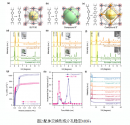
Epitaxy of wafer-scale single-crystal MoS2 monolayer via buffer layer control​

Abstract​

Monolayer molybdenum disulfide (MoS2), an emergent two-dimensional (2D) semiconductor, holds great promise for transcending the fundamental limits of silicon electronics and continue the downscaling of field-effect transistors. To realize its full potential and high-end applications, controlled synthesis of wafer-scale monolayer MoS2 single crystals on general commercial substrates is highly desired yet challenging. Here, we demonstrate the successful epitaxial growth of 2-inch single-crystal MoS2 monolayers on industry-compatible substrates of c-plane sapphire by engineering the formation of a specific interfacial reconstructed layer through the S/MoO3 precursor ratio control. The unidirectional alignment and seamless stitching of MoS2 domains across the entire wafer are demonstrated through cross-dimensional characterizations ranging from atomic- to centimeter-scale. The epitaxial monolayer MoS2 single crystal shows good wafer-scale uniformity and state-of-the-art quality, as evidenced from the ~100% phonon circular dichroism, exciton valley polarization of ~70%, room-temperature mobility of ~140 cm2v−1s−1, and on/off ratio of ~109. Our work provides a simple strategy to produce wafer-scale single-crystal 2D semiconductors on commercial insulator substrates, paving the way towards the further extension of Moore’s law and industrial applications of 2D electronic circuits.

Please, Log in or Register to view URLs content!
 

tokenanalyst

Brigadier
Registered Member

Semiconductor equipment order volume grows steadily, Amei Shanghai's revenue and net profit double in 2023​

Shengmei Shanghai disclosed its 2023 annual performance report. Its operating income in 2023 was 3.888 billion yuan, a year-on-year increase of 35.34%, and the net profit attributable to shareholders of listed companies was 911 million yuan, a year-on-year increase of 36.21%. %, net profit excluding non-recurring gains and losses was 868 million yuan, a year-on-year increase of 25.77%.
In terms of products, semiconductor cleaning equipment achieved revenue of 2.614 billion yuan, a year-on-year increase of 25.79%, and a gross profit margin of 48.62%; other semiconductor equipment (electroplating, vertical furnace tubes, stress-free copper polishing and other equipment) revenue was 940 million yuan Yuan, a year-on-year increase of 81.57%, and the gross profit margin was 59.50%; the revenue of advanced packaging wet-process equipment was 160 million yuan, a year-on-year increase of 0.09%, and the gross profit margin was 42.14%.
Shengmei Shanghai said that it is mainly due to the increasing demand for equipment in the domestic semiconductor industry, and sales orders have continued to grow; it has achieved certain results in new customer expansion and new market development; new products have been recognized by customers, and order volume has grown steadily.
In recent years, although China's semiconductor industry has been slightly affected due to macro-environment and other reasons, China is still the world's largest semiconductor consumer market. In 2023, the external environment for the development of China's integrated circuit industry will become more severe. The new export policies introduced abroad will have a great impact on China's semiconductor equipment industry, but it will also bring unprecedented opportunities, which will continue to promote the domestic or regional semiconductor industry. development of.
Since its establishment, Shengmei Shanghai has been committed to providing leading equipment and process solutions to the global integrated circuit industry, adhering to the development strategy of differentiated international competition and original innovation, and established a relatively complete intellectual property system through independent research and development. Rich technology and process accumulation have formed internationally leading front-end semiconductor process equipment, including cleaning equipment (including single-chip, trough, single-chip trough combination, CO2 supercritical cleaning, edge and back scrubbing), semiconductor electroplating equipment , vertical furnace tube series equipment (including oxidation, diffusion, vacuum tempering, LPCVD, ALD), front-end glue coating and development Track equipment, plasma enhanced chemical vapor deposition PECVD equipment, stress-free polishing equipment/back-end advanced packaging process equipment As well as silicon material substrate manufacturing process equipment, etc.

Please, Log in or Register to view URLs content!
 

tokenanalyst

Brigadier
Registered Member

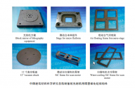
Silicon carbide ceramic precision parts , inject soul into the new generation of lithography machine.​

1709215820505.png

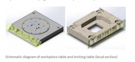
Generally speaking, the workpiece table structure for lithography machine shall meet the following requirements:

① High lightweight: in order to reduce the motion inertia, reduce the motor load, and improve the motion efficiency, positioning accuracy and stability, lightweight structural design is widely used for structural parts, with a lightweight rate of 60% - 80%, up to 90%;

② High form and position accuracy: in order to achieve high-precision movement and positioning, structural members are required to have extremely high form and position accuracy, and the flatness, parallelism and perpendicularity are required to be less than 1 μ m. The shape and position accuracy shall be less than 5 μ m;

③ High dimensional stability: in order to achieve high-precision movement and positioning, structural members are required to have high dimensional stability, which is not easy to produce strain, and high thermal conductivity, low thermal expansion coefficient, which is not easy to produce large dimensional deformation;

④ Clean and pollution-free: structural members are required to have extremely low friction coefficient, small kinetic energy loss during movement, and no pollution of grinding particles.

● silicon carbide ceramic square mirror

The key components in the key equipment of integrated circuits such as lithography machine have the characteristics of complex shape, complex overall dimension and hollow lightweight structure, so it is difficult to prepare such silicon carbide ceramic components. At present, the international mainstream integrated circuit equipment manufacturers, such as ASML in the Netherlands, Nikon and Canon in Japan, use a large number of microcrystalline glass, cordierite and other materials to prepare the core component of the lithography machine - square mirror, and use silicon carbide ceramics to prepare other simple shape high-performance structural components. However, the experts of China Academy of building materials science have adopted proprietary preparation technology to realize the preparation of large-size, complex shape, highly lightweight, fully enclosed silicon carbide ceramic square mirrors and other structural and functional optical components for lithography.

1709215988955.png

Please, Log in or Register to view URLs content!
 

tokenanalyst

Brigadier
Registered Member

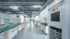
Sirius Semiconductor Shanghai Automotive Grade Reliability Experiment Center was officially opened​


Recently, Sirius Semiconductor officially announced the official opening of the Shanghai Automotive Grade Reliability Experiment Center.

It is understood that Shenzhen Tianlangxin Semiconductor Co., Ltd. will set up a vehicle-grade reliability experiment center in Jiading District, Shanghai at the end of 2023. This experimental center is an open experimental platform for power devices that Tianlangxin Semiconductor focuses on building and building. The business is the reliability experiment and verification of automotive-grade power devices (MOSFET, SiC, GaN, IGBT single tube + module), and is committed to providing reliability testing and certification reports to Tianlangxin’s customers.

1709218699461.png

The total area of the laboratory is about 700 square meters, with an investment of more than 10 million yuan in the first phase. The laboratory team consists of about ten engineers and experimenters, and is equipped with advanced high-precision reliability testing equipment at home and abroad. The experimental projects are completely Implemented in accordance with AEC-Q101 certification standards, the fifteen experimental projects in the first phase have been fully operational.
Currently available projects include: Highly Accelerate Atress Test, High Humidity High Temp. Reverse Bias, Autoclave, Temperature Cycling, High Temperature Storage, Temperature Humidity Test, intermittent service life Intermittent Operational Life, High Temperature Reverse Bias, High Temperature Gate Bias, Scanning Acoustic Microscope, etc.
Tianlang Core Automotive Grade Reliability Laboratory has established a sound operating process and service system, and strictly follows the CNAS (China National Accreditation Service for Conformity Assessment) ISO/IEC17025:2017 standard guidance and certification. At present, the laboratory has launched a coaching institution to enter the laboratory. process, it is expected to complete the CNAS coaching and certification work in early 2025.

Please, Log in or Register to view URLs content!
 

tokenanalyst

Brigadier
Registered Member

Wuhan’s compound semiconductor project settles in Optics Valley​


According to the "China Optics Valley" report, on February 27, the high-end compound semiconductor materials and chip industrialization base project of Leading Technology Group Co., Ltd. (hereinafter referred to as Leading Technology Group) was signed and landed in Wuhan Optics Valley. Lead Technology Group stated that the company will accelerate project construction, increase scientific research cooperation with Wuhan universities and colleges, and promote continuous new breakthroughs in semiconductor material research and development.

Lead Technology Group has functional materials division, infrared laser division, compound semiconductor division, thin film materials division, etc. Its products are widely used in aerospace, artificial intelligence, semiconductors, microelectronics, new energy, 5G, optical communications, photovoltaics , LED lighting, new displays, electronics, medicine and medical care, animal nutrition and other high-growth industries.

Among them, the Compound Semiconductor Division provides microelectronic and optoelectronic application products including III-V compound semiconductor substrates (GaAs, InP), Ge semiconductor substrates, metal organic sources, special gases, PBN ceramics and high-purity metals.
Please, Log in or Register to view URLs content!
 

tokenanalyst

Brigadier
Registered Member

New progress in room temperature synthesis of stable mesoporous metal-organic framework materials​


Stable mesoporous metal-organic frameworks (MOFs) have high specific surface area, large pore size (2-50 nm) and structure controllability, and are widely used in catalyst loading, adsorption, separation and other fields. However, most MOFs reported so far are microporous ( pore diameter less than 2 nm) , and the proportion of mesoporous MOFs is less than 1% . At the same time, most mesoporous MOFs have insufficient stability. The synthesis of stable MOFs usually requires high temperature and strong acid environment, and it is impossible to coat unstable functional molecules ( such as enzymes, quantum dots, metal complexes, some heteropolyacids, etc. ) in situ . Therefore, developing synthetic strategies for stable mesoporous MOFs under mild conditions ( room temperature, neutral solvent ) is a challenging task. Recently, Professor Yuan Shuai and Professor Zuo Jinglin of Nanjing University collaborated with Zheng He and others to break through the problem of synthesizing stable mesoporous MOFs at room temperature and neutral conditions, and achieved in-situ stable coating and synergy of multiple functional molecules. catalytic.

The growth conditions of MOFs are usually determined by the strength of coordination bonds. Stable MOFs based on high-valent metals (such as Zr-MOFs ) usually require high temperatures and acidic regulators to generate crystalline products, while unstable MOFs based on low-valent metals can be grown at room temperature. Single crystals are formed in neutral solvents. In view of this, the team developed a dynamic chemical bond-directed synthesis method to obtain single crystals of stable mesoporous Zr-MOFs under mild conditions . First, a MOFs template with stable Zr carboxyl coordination bonds and unstable Cu -pyridine groups was constructed . Since the synthesis reaction was performed at room temperature, kinetic products with mesopores could be isolated, avoiding the generation of thermodynamically stable microporous MOFs . . Subsequently, through the single crystal to single crystal transformation process, the unstable Cu- pyridine ligands are replaced by linear organic ligands with similar lengths and stability, forming stable single crystals of mesoporous MOFs . Two new iso-mesh reo topology MOFs were successfully constructed using this strategy , namely Compound 1′ and Compound 2′ . Among them, Compound 1′ has higher porosity (N 2 adsorption capacity is 1045 cm 3 g -1 ) , larger pore size (2.5 nm) and higher chemical stability (pH value 1-11) . In addition, a series of acid-sensitive materials, including POM , CdSeS/ZnS quantum dots, and metal coordination cages, were successfully encapsulated in Compound 1′ . Among them, POM@compound 1′ has high catalytic activity for the degradation of VX . This article reports the application of dynamic chemical bond-guided synthesis of mesoporous stable MOFs and in-situ encapsulation of nanofunctional materials at room temperature, providing new ideas for the research on the synthesis of stable MOFs and MOF- based composite materials.

1709243970664.png

Please, Log in or Register to view URLs content!
 

tokenanalyst

Brigadier
Registered Member

A temperature control algorithm for lithography machine based on generalized predictive control and BP neural network PI control.​


Abstract​

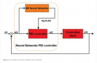
Temperature stability is a critical factor affecting the performance of the most subsystems in the lithography system, due to the high precision and sensitivity of system components to temperature variations. The temperature control system of the lithography machine is characterized by its large inertial constant, time delay characteristics, as well as susceptibility to multiple disturbances. The temperature control system of the lithography machine chiefly requires response speed, high accuracy, and stable and constant temperature control. The contribution of this study is not only avoiding complex precision modeling processes based on real-time parameter estimation and neural network self-tuning but also improving the performance of temperature control in real time under external disturbances. A novel adaptive algorithm with a cascade structure based on generalized predictive control (GPC) and backpropagation (BP) neural network proportional-integral (PI) control is successfully proposed for high accuracy temperature control of lithography machine with a large inertial constant, time delay, and multiple disturbances. In this study, firstly, the liquid circulating temperature control system is developed based on heat exchanger and heater. Secondly, an adaptive controller composed of GPC and BP neural network PI control is successfully proposed.
A BP neural network is employed to enable the parameters of the PI controller to adjust in real time, and the mathematical model parameters of the control system are identified in real time by the least square method. Also, the performance of the proposed controller is evaluated comparing with conventional PI controller and GPC controller in terms of robustness and quantitative study of error analysis. Finally, the temperature stability and robustness of the temperature control system controlled with the proposed adaptive GPC-PI algorithm has been investigated by the simulation results carried out in different working scenarios. The simulation results show that the steady-state error from the proposed algorithm is less than 0.01°C under the action of disturbance input. It can effectively counteract the influence of environmental interference and time-varying system parameters. The results of the simulation experiment indicate that the proposed adaptive GPC and PI control algorithm exhibits significant advantages in terms of control accuracy, anti-interference ability, and robustness compared to the conventional control method.​

1709247256107.png

Please, Log in or Register to view URLs content!
 

tokenanalyst

Brigadier
Registered Member

Sirui Intelligent successfully completed hundreds of millions of yuan in Series B financing​


Qingdao Sifang Sirui Intelligent Technology Co., Ltd. (Sirui Intelligence) announced through its official WeChat public account that it has recently completed hundreds of millions of yuan in Series B financing. This round of financing was jointly led by SAIC Strategic Direct Investment, Shangqi Capital and CDH Investment; well-known investors such as China Merchants Venture Capital, Shanghai Gimpo, Xinding Capital, Sinovation Ventures, Huakong Fund and Qing Venture Capital also participated in the investment; Old shareholders such as Ocean Pine Capital, Haiao Xinke, Xinxin Venture Capital, Hengchuang Investment, and Tongge Venture Capital continue to support the company. The successful completion of this important financing milestone benefited from the strong support and high recognition of the company's partners and new and old shareholders.

1709249758291.png

According to reports, Sirui Intelligent focuses on the R&D, production and sales of key semiconductor front-end process equipment, and provides system equipment products and technical service solutions with independently controllable core key technologies. At present, Sirui Intelligent has formed a "dual main business" layout. The company's products include atomic layer deposition (ALD) equipment and ion implantation (IMP) equipment. It is widely used in many high-precision fields such as integrated circuits, third-generation semiconductors, new energy, optics, and parts coating.


Please, Log in or Register to view URLs content!
 
Top