Chinese semiconductor thread II

tokenanalyst

Brigadier
Registered Member

Huafeng Testing & Control will achieve revenue of 905 million yuan in 2024, a year-on-year increase of 31.05%.​


Huafeng Testing & Control released its 2024 annual performance report, stating that the company's operating income for the year reached 905,345,386.04 yuan, a year-on-year increase of 31.05%; the net profit after deducting non-recurring gains and losses was 340,047,435.55 yuan, a significant year-on-year increase of 34.35%, and the performance has stabilized and recovered.

the company's core product STS8300 performed well, with shipments increasing significantly year-on-year, and the customer ecosystem construction has begun to show results. This series of achievements fully demonstrates the company's strong competitiveness and development potential in the wave of industry recovery, and has effectively promoted the double growth of operating income and net profit during the reporting period compared with the same period last year.

As of the end of the reporting period, the company has applied for 397 intellectual property rights, of which 249 have been authorized. During the reporting period, the company's R&D investment was RMB 172,368,197.98, an increase of 30.60% over the same period last year, accounting for 19.04% of the company's operating income. The size of the R&D team continued to expand, with 379 R&D personnel, accounting for 48.59% of the company's total employees.

Regarding the reasons for the performance changes in 2024, Huafeng Measurement & Control explained that during the reporting period, the industry structure has undergone positive changes. After the inventory adjustment in 2023, the semiconductor industry showed a good trend of moderate recovery in 2024. At the same time, the domestic economy has gradually stabilized, and the downstream market demand has increased accordingly.

Please, Log in or Register to view URLs content!
 

tokenanalyst

Brigadier
Registered Member

Jinghe Integrated's Phase III project implementation entity increased capital to 9.59 billion​


Hefei Wanxin Integrated Circuit Co., Ltd. recently underwent industrial and commercial changes, adding China Construction Bank Financial Asset Investment Co., Ltd., Bank of Communications Financial Asset Investment Co., Ltd., and ICBC Investment's ICBC Financial Investment Emerging Industries Equity Investment Fund Partnership as shareholders. The registered capital increased from approximately 50 million yuan to approximately 9.59 billion yuan, and several senior executives also changed.

It is understood that Hefei Wanxin Integrated Circuit Co., Ltd. was established in December 2022. It is a wholly-owned subsidiary of Jinghe Integrated Circuit and the main body of the construction of Jinghe Integrated Circuit Phase III project. The total investment of Jinghe Integrated Circuit Phase III project is 21 billion yuan. It plans to build a 12-inch wafer manufacturing production line with a production capacity of about 50,000 pieces/month, focusing on the layout of 55nm to 28nm display driver chips, 55nm CMOS image sensor chips, 90nm power management chips, 110nm microcontroller chips and 28nm logic chips. Product applications cover market areas such as consumer electronics, automotive electronics and industrial control.

Previously, Jinghe Integrated Circuit stated in an announcement that the capital increase was to enhance the comprehensive competitiveness of Wanxin Integrated Circuit in integrated circuit project research and development, market expansion, product mass production, etc., and to optimize the capital structure. The capital increase funds will be mainly used for the daily operations of Wanxin Integrated Circuit, including but not limited to the purchase of equipment and repayment of debts related to the production and operation of the main business.

Please, Log in or Register to view URLs content!
 

tokenanalyst

Brigadier
Registered Member

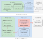
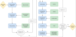
An Efficient Machine Learning-Enhanced DTCO Framework for Low-Power and High-Performance Circuit Design.​

Abstract​

The standard Design Technology Co-Optimization (DTCO) involves frequent interactions between circuit design and process manufacturing, which requires several months. To assist designers in establishing a bridge between device parameters and circuit metrics efficiently, and provide guidance for parameter optimization in the early stages of circuit design. In this paper, we propose an efficient machine learning (ML)-enhanced DTCO framework. This framework achieves the co-optimization of device parameters and circuit metrics. We select the gate metal work function (WF) as the parameter to validate the effectiveness of our framework. And the ridge regression approach is used to bypass TCAD simulation, compact model extraction and cell library characterization. We reduces time consumption by at least 92% compared to traditional DTCO framework, while ensuring that errors of delay, internal power consumption and leakage power below 4ps, 0.035mJ, and 0.4uW, respectively. By adjusting the WF, we achieved a better balance between circuit delay and power consumption. This work contributes to designers exploring a broader design space and achieving a efficient DTCO flow.​

1741964912710.png1741964574730.png
Please, Log in or Register to view URLs content!
 

tokenanalyst

Brigadier
Registered Member
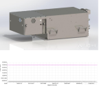
RSLASER making progress on the commercialization MHZ range Solid State DUV Source, we could see more DUV maskless lithography.

High-end deep ultraviolet quasi-continuous solid laser light source achieves domestic substitution

Deep ultraviolet quasi-continuous solid laser light sources have a wide range of application scenarios and have unique technical advantages in material surface detection (semiconductor wafer defect detection, etc.), laser induced breakdown spectroscopy ( LIBS) , laser induced fluorescence ( LIF ), ultraviolet Raman spectrometer, laser fine micromachining (laser direct writing, laser induced plasma processing, optical Bragg grating writing), etc. These applications have similar requirements for light sources: short wavelength, narrow spectral linewidth, high power, good repetition frequency, high stability and high reliability.

With the increasing demand for high-end deep ultraviolet light sources in the 266nm and below bands in China , there are procurement risks for imported light sources with a monopoly position abroad , and it is difficult to guarantee the after-sales timeliness of the products. Domestic related industries are in urgent need of domestic substitution of high-end deep ultraviolet light sources . In this context, Beijing Keyi Hongyuan Optoelectronics Technology Co., Ltd. (hereinafter referred to as Keyi Hongyuan ) actively carries out scientific research and breakthroughs in many key core technical difficulties using the existing optical, mechanical, electrical , control, and measurement complete R&D systems , forming high-end deep ultraviolet light source products with high stability and reliability . This series of products has completely independent intellectual property rights and can achieve domestic substitution of high-end deep ultraviolet light sources .

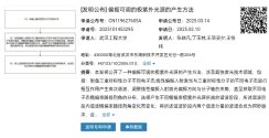
Keyi Hongyuan has launched a variety of deep ultraviolet shelf products, mainly concentrated in the 2.13 nm and 2.66 nm bands. It has developed 4 mature models with pulse widths less than 10 ps , spectral line widths less than 15 pm , and repetition frequencies of 1MHz /70MHz . The technical parameters are comparable to those of high-end deep ultraviolet light sources of imported products . Among them, the high - repetition-rate, high-power picosecond solid- state laser light source in the 266nm band has been successfully launched on the market, and commercial orders have been formed in the semiconductor testing industry and the laser fine micro-machining industry.​

1741966365119.png

Since the single photon energy of deep ultraviolet laser is high, nonlinear crystals are easily damaged, and ensuring long-term reliability is a challenge. Keyi Hongyuan independently develops and designs power stability control algorithms with independent intellectual property rights, fully automatic point shifting, high beam quality design, purge filter protection design, etc. to ensure the long-term reliability and stability of products, meet the actual needs of industrial users for long-term reliability, and has reached the world's advanced level: single-point life can achieve continuous operation for more than 1,000 hours, 1,000- hour average power RMS < 0.5 % , and beam quality M² less than 1.2 , which has surpassed the level of similar imported products.

At the same time, Keyi Hongyuan is actively developing the same type of higher repetition rate 120MHz deep ultraviolet high-power industrial-grade solid laser light source, and in response to the actual needs of more types of industrial users, it has carried out the research and development of 266nm high-power solid lasers with tunable pulse width of 2-7ns and tunable frequency of 1Hz - 1MHz . At present , the above models have completed the scheme verification and process finalization, and are in the process of product production. They will soon form shelf products and be put on the market, providing more choices for domestic industrial users of high-end deep ultraviolet light sources.

In addition to the deep ultraviolet quasi-continuous lasers in the 266 nm and below bands introduced above , Keyi Hongyuan has also developed multiple laser product series in other bands , including 532nm , 355nm and other products that meet the needs of industrial customers for high reliability and long-term stability, and the technical indicators have reached the domestic advanced level . As a domestic high-end laser manufacturer, the company has conducted in-depth communication with customers to understand customer pain points, improve customer satisfaction and user experience, provide professional customized products, and ensure product quality and delivery cycle while meeting technical indicator requirements.​
 

tokenanalyst

Brigadier
Registered Member

Xidian University created silicon-terminated diamond devices achieve kV-level breakdown voltage!​


Recently, the team of Academician Hao Yue from Xidian University has once again received important news! The research group of Professor Zhang Jincheng and Professor Zhang Jinfeng has made breakthrough progress in the field of ultra-wide bandgap semiconductor diamond power devices , and the relevant research results have been published in the top international journal "IEEE Electron Device Letters".
This achievement not only marks that China's technological strength in the field of diamond semiconductors has reached a new level, but also provides a new technical path for the development of future high-voltage and high-efficiency power electronic systems. Diamond is known as the "ultimate semiconductor" material. Due to its ultra-wide bandgap (5.5 eV), extremely high breakdown field strength (13 MV/cm) and excellent thermal conductivity (22 W/cm·K), it exhibits unparalleled advantages in electronic device applications under high voltage, high power, high temperature and extreme environments.
1741971085693.png

However, the development of diamond power devices has always faced two major challenges: low threshold voltage and voltage resistance bottleneck. These problems have seriously restricted the practical application of diamond in high-performance power electronic systems. Breakthrough innovation: Silicon/hydrogen terminal composite structure Professor Zhang Jinfeng's research team innovatively proposed a new device structure of silicon/hydrogen-terminated diamond composite conductive channel. This design cleverly combines the high interface quality of silicon-terminated diamond and the high conductivity characteristics of hydrogen-terminated diamond, successfully achieving a breakthrough in enhanced diamond high-voltage field-effect transistors.​

Please, Log in or Register to view URLs content!
 
Top