Chinese semiconductor thread II

tokenanalyst

Brigadier
Registered Member

Self-developed domestic formic acid reflux machine is in stable mass production and leading customers have verified its reliable quality.​


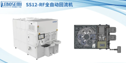
Recently, another fully automatic formic acid reflow machine independently developed by Rabo Microelectronics has been successfully shipped. With its excellent performance, it has won quality praise and brand trust from leading customers in the advanced packaging industry.

At present, our company's fully automatic formic acid reflux machine has achieved large-scale stable mass production and has been successfully deployed and applied at customer sites, demonstrating strong market adaptability and technical maturity.

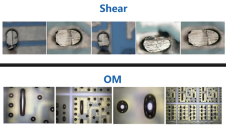
Compared with traditional flux reflow, the formic acid reflow process has low cost, no need to coat or clean flux, high production capacity, WPH ≥ 50, higher yield, no introduced impurities, and is more environmentally friendly.

The fully automatic formic acid reflow machine developed by Rabo Microelectronics is suitable for the formic acid reflow process of 12/8/6-inch wafers. The Pin & Chuck has an independent motion structure, and the recipe adjustment is more flexible. It is equipped with a fully automatic liquid replenishment and liquid supply system, and the process chamber has efficient sealing. There is also an automatic chamber opening mode, which makes maintenance operations safer and more convenient.

The equipment is mainly used for advanced packaging bump reflow, including C4/C2 bump, ubump reflow and FC welding processes, and is suitable for common solders such as pure tin, tin-silver and indium.
1741884298085.png1741884313266.png

Please, Log in or Register to view URLs content!
 

tokenanalyst

Brigadier
Registered Member

Saiwei Electronics: OEM MEMS micromirrors, opening up new areas of automotive sensing​


picture

Beijing Saiwei Semiconductor Co., Ltd. (hereinafter referred to as the "Company" or " Saiwei Semiconductor ")'s holding subsidiary, Selex Microsystems Technology (Beijing) Co., Ltd. (hereinafter referred to as "Selex Beijing"), signed a "Strategic Cooperation Framework Agreement" with an internationally renowned lidar manufacturer and its subsidiaries (hereinafter referred to as "cooperative customers") to carry out long-term strategic cooperation on MEMS micromirror products for automotive lidar. The parties will carry out comprehensive technical cooperation. Selex Beijing will be committed to establishing and maintaining an 8-inch wafer mass production production line for MEMS micromirror products based on the process requirements provided by cooperative customers, and provide supporting and stable production capacity according to the production capacity requirements of cooperative customers.

Please, Log in or Register to view URLs content!
 

tokenanalyst

Brigadier
Registered Member

Hefei's 55 billion 8.6-generation OLED project has made new progress​


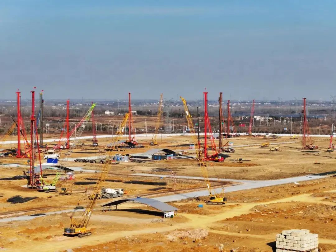
On March 10, according to Da Wan News, Hefei Guoxian's 8.6th generation AMOLED production line project has completed more than 35,000 pile foundation operations and has entered the main plant construction phase. In addition, the construction of civil engineering project B project housing, integrated power station and other projects were recently awarded to Shanghai Baoye, and the relevant construction units have entered the site for construction.
picture


It is reported that the total investment of Hefei Guoxian's 8.6th generation flexible AMOLED production line project is 55 billion yuan, with a designed production capacity of 32,000 glass substrates (size 2290mm×2620mm) per month, and construction will start in September 2024. The production line is funded by Visionox and Hefei Investment Platform, and Hefei Guoxian (a subsidiary of Visionox) is responsible for the investment, construction and operation of the production line.

As the world's first 8.6-generation AMOLED production line that adopts FMM-free (fine metal mask) technology (i.e. ViP technology), its products cover medium-sized application areas such as tablets, laptops, and automotive displays.

Visionox said that ViP technology can significantly improve the performance of AMOLED products, increasing the effective light-emitting area (aperture ratio) of AMOLED from the traditional 29% to 69%, and increasing the pixel density to more than 1,700 ppi. Combined with Tandem stacking device technology, it can achieve 6 times the device life or 4 times the brightness compared to FMM AMOLED.

Please, Log in or Register to view URLs content!
 

tokenanalyst

Brigadier
Registered Member

Vibration-resistant full-field heterodyne long-arm interferometry.​

Abstract​

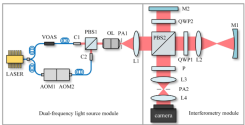
Long-distance surface profiling requires a high level of vibration resistance. Here, we propose a heterodyne interferometry scheme that uses two acousto-optic modulators (AOMs) to achieve precise and high-speed heterodyne phase-shifting frequencies. This solution offers high spatial resolution and effective vibration resistance. We measured the fundamental vibration conditions in the laboratory and simulated the effect of vibration on measurement repeatability across different difference frequencies. Experiments have demonstrated that this method can produce a single 3200 Hz sampling of a 1024 pixel × 1024 pixel camera within a period of 1.25 ms. The repeatability of measurements at 22 m away is better than 0.8‰ wave root mean square (RMS).​

1741893721992.png1741893812395.png

Please, Log in or Register to view URLs content!
 

tokenanalyst

Brigadier
Registered Member

Piotech: Shipped more 1000 deposition chambers in 2024 and hybrid bonding products are used in mass production.​


The shipment of equipment reaction chambers exceeded 1,000, and the main product PECVD received repeat purchases and bulk orders from customers. In 2024, the company shipped more than 1,000 equipment reaction chambers, setting a historical annual high. The mass production scale of a series of products such as PECVD, ALD, SACVD, HDPCVD, Flowable CVD and hybrid bonding equipment continues to expand, and continues to obtain customer orders. In terms of thin film deposition equipment, (1) 24H1 PECVD received repeat purchases and bulk orders from customers. (2) The verified Thermal-ALD received repeat orders again; PE-ALD high-temperature and low-temperature SiO2, SiN, etc. have been shipped to customers for verification. (3) As of 24H1, the cumulative shipments of HDPCVD reaction chambers reached 70. In terms of hybrid bonding equipment, 24H1's wafer-to-wafer bonding product Dione 300 and chip-to-wafer hybrid bonding front surface and processing product Propus both received repeat orders from customers for mass production.​
 

tokenanalyst

Brigadier
Registered Member

China’s first 12-inch smart sensor wafer manufacturing production line project passed completion acceptance!​


Recently, the Guangzhou Zengxin 12-inch advanced intelligent sensor wafer manufacturing mass production line project undertaken by China Construction Fourth Engineering Bureau successfully passed the completion acceptance.

The project is located in Zengcheng District, Guangzhou City, Guangdong Province, with a total construction area of about 200,000 square meters. The construction content includes production plants, integrated power stations, silane stations, Class A warehouses, hazardous waste warehouses, bulk gas stations, production dispatching buildings, etc.

As the first 12-inch intelligent sensor wafer manufacturing production line project in the country, it will have an annual production capacity of 240,000 12-inch wafers after completion. After commissioning, the products produced are mechanical, acoustic, microfluidic, biological and other sensor devices and supporting ASIC chips, which will gradually form an industrial agglomeration effect, provide high-quality development support for domestic intelligent sensors and related industries, and help the construction of the “Guangdong Strong Core” project.

Please, Log in or Register to view URLs content!
 

OptimusLion

Junior Member
Registered Member
Han's Semiconductor East China Headquarters Project Signed in Suzhou High-tech Zone

Semiconductor Industry Network learned that on March 13, the East China Headquarters Project of Han's Semiconductor was signed in Suzhou High-tech Zone. Wu Qi, deputy secretary of the District Party Working Committee and mayor of the District Government, met with Zhang Jianqun, vice chairman and executive vice general manager of Han's Laser Technology Industry Group Co., Ltd. and witnessed the signing together.

Yin Jiangang, deputy general manager of Han's Laser Technology Industry Group Co., Ltd. and chairman of Shenzhen Han's Semiconductor Equipment Technology Co., Ltd.; district leaders Shen Yan and Yang Liang, and relevant persons in charge of district-related departments, sectors, and state-owned enterprises attended the event. Han's Laser Group was established in 1996 and is a listed company on the main board of the Shenzhen Stock Exchange. It is also the largest industrial laser processing equipment manufacturer in Asia and one of the top three in the world. It has established more than 100 R&D, production and sales outlets in 15 countries around the world.

The Han's Semiconductor Division is affiliated to the Han's Laser Group, and mainly focuses on providing a series of automated professional equipment from fine micro-machining to visual inspection for industries such as LED, panel, and semiconductor. This time, Han's Semiconductor plans to establish its East China headquarters in the High-tech Zone, mainly engaged in the research and development, production and sales of coating, developing and cleaning equipment.

During the meeting, Wu Qi said that the High-tech Zone has been committed to building an internationally competitive photonics and integrated circuit industry cluster. The addition of Han's Semiconductor will inject strong momentum into the development of related industries in the High-tech Zone and even the entire East China region. We will go all out to promote project construction, provide comprehensive services and support, and jointly create a new chapter of mutual benefit and win-win results.

Zhang Jianqun said that the Hi-Tech Zone has a complete layout of the photonic and integrated circuit industry chain, rich innovation resources and a superior policy environment. In the future, Han's Semiconductor will rely on its East China headquarters, focus on core technology areas, increase R&D investment, optimize product structure, and provide the most advanced and efficient solutions for semiconductor manufacturing companies in the Hi-Tech Zone and even the whole country.

IMG_20250314_084549_179.jpg

Please, Log in or Register to view URLs content!
 

OptimusLion

Junior Member
Registered Member
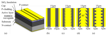
Changchun Institute of Optics, Fine Mechanics and Physics optimizes and fabricates high-brightness HiBBEE inhomogeneous waveguide semiconductor laser

High-brightness semiconductor lasers have extremely important applications in fields such as laser radar. Traditional semiconductor lasers face difficulties such as large vertical divergence angle, elliptical beam output, multiple lateral modes, and poor beam quality, which limit the direct application of high-brightness semiconductor lasers.

To address this problem, the team of the Bimberg Sino-German Green Photonics Research Center of the Changchun Institute of Optics, Fine Mechanics and Physics adopted a high-brightness vertical wide-area edge emission (HiBBEE) structure in the vertical direction, using the photonic bandgap effect to replace the traditional total reflection principle to limit the light field, increase the size of the light mode, and reduce the vertical divergence angle of the semiconductor laser; at the same time, in the lateral direction, a non-uniform waveguide was used to suppress the lateral high-order mode, improve the lateral beam quality of the semiconductor laser, and optimize the design and prepare the HiBBEE non-uniform waveguide semiconductor laser . The vertical and lateral divergence angles are still as low as 8.6° and 5.1° at a current of 1.5A, and the fundamental mode output is maintained, with a brightness that is 1.5 times higher than that of similar devices.

This high-brightness HiBBEE inhomogeneous waveguide semiconductor laser can significantly reduce the application cost of semiconductor lasers and has broad application prospects.


083459582 (1).png

083459202.png


Please, Log in or Register to view URLs content!
 
Top