Chinese semiconductor thread II

tokenanalyst

Brigadier
Registered Member
Multi-electron beam focusing device and control method

View attachment 147815
Interesting and game changing, this patent is for a Multibeam Mask Writer.

CN212648184U

Background.

Improving the productivity of electron beam exposure machines can be achieved by increasing the scanning speed. However, the current scanning speed of single-beam scanning electron beam exposure machines is already between 50MHz and 100MHz, and there is very limited room for improvement. Although increasing the electron beam current is also a solution, the cost is that the beam spot of the electron beam increases, and the resolution of the system decreases, which is not worth the loss. The most effective way is to increase the number of electron beams. A large number of electron beams are processed in an array manner, which is much more efficient than a single point source exposure. The RIKEN Institute of Physical and Chemical Research in Japan began the development of multi-beam electron beam exposure machines around 1980, and a small number of units in the world have also carried out research on multi-beam parallel exposure technology. However, with the gradual clarity of the prospects of deep ultraviolet (DUV) and extreme ultraviolet (EUV) technologies and their mass production capabilities, mainstream technology is not optimistic about the prospects of multi-beam electron beam exposure machines, so they have developed slowly over the years.

Currently, IMS Nanofabrication is the only company that provides commercial multi-beam electron beam exposure machines, but it is limited to using 260,000 sub-beams to make a line width of 30 nanometers for the production of integrated circuit optical exposure masks at the 7-nanometer node (the beam spot of each sub-beam of the company's machine can only be focused to 20 nanometers). The Dutch company Mapper is currently developing its third-generation system FLX, dedicated to the development of a 650,000 sub-electron beam system, trying to achieve a yield of 40 12-inch wafers per hour at the 28-nanometer node. Unfortunately, Mapper declared bankruptcy at the end of 2018 due to funding problems, and the prospects of FLX are unknown.

Even so, multi-beam electron beam exposure machines still have huge market prospects. At present, the one-time investment cost of deep ultraviolet and extreme ultraviolet lithography machines is high. For example, the price of an immersion DUV lithography machine that can meet the 14-nanometer node is more than 75 million US dollars. A set of optical masks required for lithography patterning costs about 10 million US dollars. Such a high investment greatly limits the technological development of application-specific integrated circuits, such as Internet of Things chips and artificial intelligence chips. Multi-beam electron beam exposure machines are low in cost. If the yield of 20-30 8-inch chips exposed per hour can be achieved, it will promote the rapid improvement and production of Internet of Things chips and artificial intelligence chips, and form a new semiconductor industry ecology. Generally speaking, there are several ways to achieve multi-beam electron beams:

Description
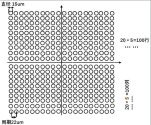
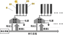
The utility model discloses a multi-electron beam focusing device. The electron beam generated by the electron beam emission source is sequentially split by a beam splitter, an accelerating lens is used to increase the energy of the electron beam, a phase-defocusing lens is used to eliminate the phase difference to improve the quality of the electron beam, an objective lens array is used to focus the beam spot of each electron beam to improve the resolution, and after the electron beam position is fine-tuned by an electron beam deflector, the electron beam is turned on or off by a beam gate, thereby improving the resolution of the electron beam. In addition, each electron beam has a dedicated electron optical system, a deflection system and a beam gate, so as to facilitate the precise control of the electron beam. Therefore, a larger number of electron beams can be accommodated on a wafer of the same area to achieve simultaneous exposure, thereby improving the accuracy and speed in integrated circuit processing applications.

1741984677886.png1741984705425.png


sunnymaxi

Major
Registered Member
Interesting and game changing, this patent is for a Multibeam Mask Writer.

CN212648184U

Background.

Improving the productivity of electron beam exposure machines can be achieved by increasing the scanning speed. However, the current scanning speed of single-beam scanning electron beam exposure machines is already between 50MHz and 100MHz, and there is very limited room for improvement. Although increasing the electron beam current is also a solution, the cost is that the beam spot of the electron beam increases, and the resolution of the system decreases, which is not worth the loss. The most effective way is to increase the number of electron beams. A large number of electron beams are processed in an array manner, which is much more efficient than a single point source exposure. The RIKEN Institute of Physical and Chemical Research in Japan began the development of multi-beam electron beam exposure machines around 1980, and a small number of units in the world have also carried out research on multi-beam parallel exposure technology. However, with the gradual clarity of the prospects of deep ultraviolet (DUV) and extreme ultraviolet (EUV) technologies and their mass production capabilities, mainstream technology is not optimistic about the prospects of multi-beam electron beam exposure machines, so they have developed slowly over the years.

Currently, IMS Nanofabrication is the only company that provides commercial multi-beam electron beam exposure machines, but it is limited to using 260,000 sub-beams to make a line width of 30 nanometers for the production of integrated circuit optical exposure masks at the 7-nanometer node (the beam spot of each sub-beam of the company's machine can only be focused to 20 nanometers). The Dutch company Mapper is currently developing its third-generation system FLX, dedicated to the development of a 650,000 sub-electron beam system, trying to achieve a yield of 40 12-inch wafers per hour at the 28-nanometer node. Unfortunately, Mapper declared bankruptcy at the end of 2018 due to funding problems, and the prospects of FLX are unknown.

Even so, multi-beam electron beam exposure machines still have huge market prospects. At present, the one-time investment cost of deep ultraviolet and extreme ultraviolet lithography machines is high. For example, the price of an immersion DUV lithography machine that can meet the 14-nanometer node is more than 75 million US dollars. A set of optical masks required for lithography patterning costs about 10 million US dollars. Such a high investment greatly limits the technological development of application-specific integrated circuits, such as Internet of Things chips and artificial intelligence chips. Multi-beam electron beam exposure machines are low in cost. If the yield of 20-30 8-inch chips exposed per hour can be achieved, it will promote the rapid improvement and production of Internet of Things chips and artificial intelligence chips, and form a new semiconductor industry ecology. Generally speaking, there are several ways to achieve multi-beam electron beams:

Description
The utility model discloses a multi-electron beam focusing device. The electron beam generated by the electron beam emission source is sequentially split by a beam splitter, an accelerating lens is used to increase the energy of the electron beam, a phase-defocusing lens is used to eliminate the phase difference to improve the quality of the electron beam, an objective lens array is used to focus the beam spot of each electron beam to improve the resolution, and after the electron beam position is fine-tuned by an electron beam deflector, the electron beam is turned on or off by a beam gate, thereby improving the resolution of the electron beam. In addition, each electron beam has a dedicated electron optical system, a deflection system and a beam gate, so as to facilitate the precise control of the electron beam. Therefore, a larger number of electron beams can be accommodated on a wafer of the same area to achieve simultaneous exposure, thereby improving the accuracy and speed in integrated circuit processing applications.

View attachment 147825View attachment 147826
Patent filled date - 2020

now image the latest development and progress in 2025..
 

tokenanalyst

Brigadier
Registered Member

Yuwei Semiconductor's first mask pattern defect inspection equipment was officially shipped​


Recently, Hefei Yuwei Semiconductor Technology Co., Ltd. (hereinafter referred to as "Yuwei Semiconductor"), an investment enterprise of Hefei High-tech Investment New Economic Development Fund, officially shipped and delivered the Raptor-500, the first domestic mask pattern defect inspection equipment that meets the requirements of 90nm and above processes, to a leading domestic mask manufacturer. The equipment provides a highly competitive domestic solution for the quality control of mature process masks, marking a key breakthrough in the field of core inspection equipment for Yuwei Semiconductor.

Previously, Yuwei Semiconductor has successively released the i6R series of products (mask shipment and pre- and post-lithography quality control) and the Halo series of products (blank substrate quality control), which have gradually become benchmark equipment for related processes in the industry. The Raptor-500 shipped this time is the third core equipment for Yuwei Semiconductor's mask quality control. Raptor-500 works with i6R and Halo products to provide a "one-stop mask zero defect" solution from substrate to finished product. The Raptor product series adopts a modular architecture design with high performance, high yield and high scalability. It can share the pressure of high-cost equipment production capacity, help customers reduce operating costs, and provide value for customers' process upgrades in the long term.

1741985718145.png

Yuwei Semiconductor's headquarters was officially settled in Hefei High-tech Zone in July 2021, focusing on the research and development of semiconductor testing and measurement equipment, and is committed to providing high-precision solutions for wafer manufacturing, mask manufacturing and packaging. At present, the company has obtained a number of national-level specialized and new enterprise certifications, its products cover mainstream domestic semiconductor manufacturers, and the cumulative shipment of equipment has exceeded 100 units.


Yuwei inspection workflow.
1741985737828.png

Please, Log in or Register to view URLs content!
 

tokenanalyst

Brigadier
Registered Member
A wafer detection scattered light collection objective lens and wafer detection equipment

View attachment 147818
Nano's first dark field inspection product DF70 will be integrated and verified for customers. It is understood that the field of dark field defect inspection in China is basically monopolized by KLA. DF70, which is positioned for dark field inspection of graphic wafers, is benchmarked against the KLA Voyager series and uses deep ultraviolet DUV lasers. It can be applied to 12-inch advanced process production lines, filling the gap in the advanced process field for domestic manufacturers.
1741986978972.png
Mainstream semiconductor processes are developing from 28nm and 14nm to 10nm and 7nm. Some international advanced semiconductor manufacturers have achieved mass production of 5nm process and started research and development of 3nm process.In the future, Nano's DF product series will not only meet the production line requirements of the 7nm node, but will also be compatible with the production line requirements of the 28nm-10nm node, competing with the KLA PUMA series and achieving a comprehensive replacement of KLA products in the field of dark field inspection of graphic wafers.
 

sunnymaxi

Major
Registered Member
Nano's first dark field inspection product DF70 will be integrated and verified for customers. It is understood that the field of dark field defect inspection in China is basically monopolized by KLA. DF70, which is positioned for dark field inspection of graphic wafers, is benchmarked against the KLA Voyager series and uses deep ultraviolet DUV lasers. It can be applied to 12-inch advanced process production lines, filling the gap in the advanced process field for domestic manufacturers.
View attachment 147829
Mainstream semiconductor processes are developing from 28nm and 14nm to 10nm and 7nm. Some international advanced semiconductor manufacturers have achieved mass production of 5nm process and started research and development of 3nm process.In the future, Nano's DF product series will not only meet the production line requirements of the 7nm node, but will also be compatible with the production line requirements of the 28nm-10nm node, competing with the KLA PUMA series and achieving a comprehensive replacement of KLA products in the field of dark field inspection of graphic wafers.
Jingce Electronics delivered Bright field defect inspection tool in 2023 and received orders for advanced nodes as well.

Suzhou Sihang Semiconductor Technology Co., Ltd. delivered first 90nm-65nm Bright field defect inspection tool ''TB1000'' in 2023.. and seems like they have successfully developed 28nm and below last year.

exactly, two years ago this was the weakest Non-Litho tool category for Chinese SME companies. look how tables have turned. and don't forget bright field defect inspection equipment is the most technically difficult front-end inspection equipment.

Edit - there are two more Chinese companies delivered Bright field defect inspection tool. will talk about later
 
Last edited:

antiterror13

Brigadier
this DUV lens/Optical system Patent is from Shenzhen based company not from authorized supplier of SMEE.. interesting
@tokenanalyst as you said, we are heading towards multiple suppliers on Lithography components.

"Scary" what would happen in ~5 years time, it seems China will dominate lithography system, just like EV, Solar, HSR, etc, etc ... thanks to the US ...... Chinese govt couldn't do it without the US's "helps" ;)
 
Top