Chinese semiconductor thread II

tokenanalyst

Brigadier
Registered Member

The world's first, independently developed! The new generation of C2W&W2W hybrid bonding equipment is about to be released!.​

The world's first C2W&W2W dual-mode hybrid bonding equipment independently developed by Qinghe Wafer Group - SAB 82CWW series is about to debut! This is a technological revolution that subverts tradition, a dual evolution of "continuing Moore's Law" and "going beyond Moore's Law"!
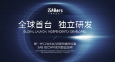
1741360471428.png

As semiconductor manufacturing processes approach the physical limit of 1nm, the continuation of Moore's Law faces huge challenges. The industry urgently needs to find new breakthroughs through the two paths of "More Moore" and "More than Moore". Whether it is 3D stacking technology to improve integration density or heterogeneous chip integration to expand functional boundaries, hybrid bonding technology has become an irreplaceable core technology. However, the traditional technology route has long faced the difficult choice between W2W (wafer to wafer) and C2W (chip to wafer): W2W pursues extreme efficiency but has high yield risk, while C2W is flexible and innovative but has low mass production efficiency.

On March 11, witness a new milestone in semiconductor bonding technology!

The SAB 82CWW series will break the technical boundaries between W2W and C2W and usher in a new era of "dual-mode parallelism"! This device not only solves the "choose one of two" dilemma that the industry has long faced, but also injects powerful momentum into AI chips, HBM storage, Micro-LED display, 3D NAND and other fields with ultra-high precision, intelligent technology and efficient production capacity, empowering future technological development!

Please, Log in or Register to view URLs content!
 

tokenanalyst

Brigadier
Registered Member


Feiling Micro launches A1, a high-performance edge-side vision AI SoC chip for AIoT applications​


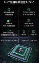
On March 7, 2025 , Flyingchip ® , a subsidiary of SmartSens, stock code 688213 , hereinafter referred to as "Flyingchip" ) , a technologically advanced intelligent visual processing chip manufacturer , recently announced the official launch of the first high-performance edge-side visual AI SoC chip in the AIoT application series - A1 . The new product A1 is equipped with high-performance AI ISP , 0.8TOPS@INT8 self-developed NPU with light computing power , 1Gb DDR3L memory and other modules, integrating excellent image processing performance and edge-side processing efficiency, low power consumption, small package size and other performance advantages. In addition, A1 can adapt to CMOS image sensors with multiple resolution specifications to form an edge-side AI SoC + Sensor system-level combination solution, which can bring high-precision, low-latency real-time intelligent images to consumer and industrial-grade intelligent vision modules and provide lightweight AI vision application operation results, accelerating the further upgrade of multiple intelligent terminal applications such as smart hardware (such as AI toys), smart homes, industrial code scanning, and night vision modules.

1741362164027.png

Please, Log in or Register to view URLs content!
 

gotodistance

New Member
Registered Member

The world's first, independently developed! The new generation of C2W&W2W hybrid bonding equipment is about to be released!.​

The world's first C2W&W2W dual-mode hybrid bonding equipment independently developed by Qinghe Wafer Group - SAB 82CWW series is about to debut! This is a technological revolution that subverts tradition, a dual evolution of "continuing Moore's Law" and "going beyond Moore's Law"!

View attachment 147249

As semiconductor manufacturing processes approach the physical limit of 1nm, the continuation of Moore's Law faces huge challenges. The industry urgently needs to find new breakthroughs through the two paths of "More Moore" and "More than Moore". Whether it is 3D stacking technology to improve integration density or heterogeneous chip integration to expand functional boundaries, hybrid bonding technology has become an irreplaceable core technology. However, the traditional technology route has long faced the difficult choice between W2W (wafer to wafer) and C2W (chip to wafer): W2W pursues extreme efficiency but has high yield risk, while C2W is flexible and innovative but has low mass production efficiency.

On March 11, witness a new milestone in semiconductor bonding technology!

The SAB 82CWW series will break the technical boundaries between W2W and C2W and usher in a new era of "dual-mode parallelism"! This device not only solves the "choose one of two" dilemma that the industry has long faced, but also injects powerful momentum into AI chips, HBM storage, Micro-LED display, 3D NAND and other fields with ultra-high precision, intelligent technology and efficient production capacity, empowering future technological development!

Please, Log in or Register to view URLs content!

Can you compare the HBM TC bonder market share #1 with the Korean semiconductor equipment company Hanmi?
 

tokenanalyst

Brigadier
Registered Member
Can you compare the HBM TC bonder market share #1 with the Korean semiconductor equipment company Hanmi?
We have to see more spec when come out. They say this machine gives a balance between High Yield and Throughput.
Hanmi is also competing against Piotech, U-Precision and other packaging equipment companies in China.
 

sunnymaxi

Major
Registered Member
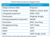
China may build the entire semiconductor supply chain in the future.
useless chart.

China has already completed the basic supply chain of entire semiconductor process from design to materials to equipment. now heading towards high end category..

and this is just the chart of mainstream Chinese firms like NAURA/AMEC/SMEE/CETC.. there is a very long list of Chinese semiconductor supply chain with minimum 2-3 companies on single equipment.. then you have NAND Flash and DRAM domestic supply chain.. basically hundreds of companies.
 
Top