Chinese semiconductor thread II

OptimusLion

Junior Member
Registered Member
Pioneer Technology's semiconductor laser radar and sensor device industrialization project is expected to be completed in October!


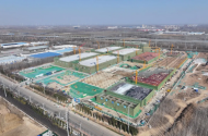
Semiconductor Industry Network learned that according to the news from Tianqu New District of Dezhou, workers are working hard at the site of Pioneer Technology's semiconductor laser radar and sensor device industrialization project. "The project is divided into two sections. After the official start of construction on August 31, 2024, there has been no stoppage for a day, and the construction period was also rushed safely and efficiently during the Spring Festival." Xie Wenting, the person in charge of the project site, said that even during the Spring Festival holiday, more than 200 workers still stick to the front line. At present, the main body of the plant in Section 1 has been capped, and the main construction of Section 2 is underway.

It is reported that laser radar and sensor components are mainly used in automotive applications such as advanced driver assistance (ADAS) and Internet of Vehicles, as well as robots, and have broad application prospects in industries such as autonomous driving, intelligent inspection, fire detection, and smart agriculture. With the gradual popularization of artificial intelligence and 5G technology, the laser radar and sensor industry will show a trend of continuous growth in technology and market size in the future. The project is located east of Chongde Eighth Avenue and south of Shangde Fifth Road in Tianqu New District, with a total investment of 5 billion yuan. It mainly builds 10 production lines, which can produce more than 10 products such as laser radar, radio frequency sensors, laser transmitting and receiving devices, and 3D modules. The project is expected to be completed in October this year, and sales revenue of 8 billion yuan can be achieved after it is put into production.
093142822.png

Please, Log in or Register to view URLs content!
 
Last edited:

OptimusLion

Junior Member
Registered Member
Jingtong Technology, which focuses on advanced packaging such as FOWLP, has received hundreds of millions of yuan in financing

Jingtong Technology has received hundreds of millions of yuan in financing, which will be mainly used for the expansion of the second phase of the packaging production line of the production base, research and development, and market investment. This round of financing was jointly invested by Lihe Capital, Da'an Fund, Anji Liangshan Guokong and Chenlong Group.

It is understood that Jingtong Technology was founded in 2018 and is headquartered in Hangzhou. It focuses on Fan-out wafer-level advanced packaging (FOWLP) and fan-out system-level advanced packaging (FOSiP) solutions, which are widely used in mobile Internet devices, high-frequency RF devices, Internet of Things (IoT), automotive, industrial and medical electronics products and other fields.

Please, Log in or Register to view URLs content!
 

OptimusLion

Junior Member
Registered Member
Xiahe Technology received tens of millions of yuan in investment to realize the localization of OLED core materials


Beijing Xiahe Technology Co., Ltd., a domestic OLED organic light-emitting material manufacturer, received tens of millions of yuan in investment from Yida Capital.

According to the official website, Xiahe Technology was established in 2017 and is a national high-tech enterprise focusing on the research and development and mass production of new OLED materials with independent intellectual property rights. With strong technical research and development capabilities and independent innovation systems, Xiahe Technology has already achieved commercial mass production of several independently developed OLED materials.


Please, Log in or Register to view URLs content!
 

tokenanalyst

Brigadier
Registered Member

Total investment of 2.1 billion yuan! Digichip Semiconductor Packaging landed in Zhejiang​


The project is invested and constructed by Zhejiang Digixin Semiconductor Co., Ltd. and is located at No. 87, Shiniu Road, Shuige Industrial Park, Lishui City, Zhejiang Province. Although Zhejiang Digixin Semiconductor Co., Ltd. was established on December 27, 2024, it is a "newcomer" in the industry, but its development potential should not be underestimated. The legal representative of the company is Chen Lei, and its business scope is wide, covering multiple key semiconductor fields such as integrated circuit manufacturing, sales and chip design services, fully demonstrating its ambition to comprehensively deploy in the semiconductor industry.

The project has many highlights, showing its high starting point and foresight. The project plans to purchase 56 acres of land, with a total construction area of 46,157 square meters. The living area, production area, office area, storage area and supporting facilities area are carefully planned. The functions are complete and the layout is scientific and reasonable, providing a solid foundation for the efficient operation of the project.

The project adopts a two-phase construction strategy. The first phase plans to invest 1.2 billion yuan, of which 1 billion yuan is used for fixed asset investment. It will purchase industrial land and factory buildings, and introduce a series of domestic and foreign advanced equipment such as silver sintering systems and vacuum ovens to build an intelligent factory and a fully automatic module factory. After the completion of the first phase of the project, it is expected to form a strong production scale of 150 million power devices per year, with an annual output value of 2.5 billion yuan, and will also contribute about 40 million yuan in taxes to the local area each year.

The second phase of the project is also exciting, with a planned investment of 900 million yuan to further expand the supporting production equipment for semiconductor modules and expand the fully automatic module factory. By then, the annual production capacity of 60 million semiconductor power devices will be added to further consolidate the project's position in the industry. The entire project construction period is from 2025 to 2027. At present, the project has made key progress. On March 4, 2025, the project filing procedures have been successfully completed, which has pressed the "accelerator" for subsequent construction. With the gradual advancement of the project, it will attract more attention and agglomeration from upstream and downstream companies in the semiconductor industry chain, forming an industrial cluster effect and driving regional economic development.

Please, Log in or Register to view URLs content!
 

tokenanalyst

Brigadier
Registered Member

Fuga Gallium Industry has made a breakthrough in gallium oxide MOCVD homoepitaxial technology, helping the downstream vertical power electronic device industry to land​


Hangzhou Fuga Gallium Technology Co., Ltd. (hereinafter referred to as Fuga Gallium), an incubated enterprise of the Hangzhou Institute of Optics and Fine Mechanics, has made important technological breakthroughs in the research and development of gallium oxide MOCVD homoepitaxial thin films. A thin film with a thickness of more than 10 microns was homoepitaxially grown on Fuga Gallium's gallium oxide single crystal substrate. Verified by national authoritative testing agencies, this technology has reached the international leading level. Related standardized products will be launched in April 2025, providing key material support for high-end equipment such as new energy vehicle high-voltage platforms and smart grid flexible transmission devices.

The test results of the third-party testing agency, China National Institute of Metrology, show that the background carrier concentration of the MOCVD epitaxial film is controlled as low as 3.6E15 cm-3, and the mobility reaches 172.7 cm2/V·s. The successful development of high-quality gallium oxide homoepitaxial film based on MOCVD technology will help the rapid implementation of the vertical high-voltage power electronic device industry above 3300V in the future.
1741349619875.png

Fuga Gallium uses MOCVD technology, based on its self-produced gallium oxide substrate products, and through substrate surface optimization, multi-step epitaxial growth and other process strategies, it has greatly improved the crystal quality and thickness of the epitaxial film, and achieved gallium oxide homoepitaxial films with low background carrier concentration and high mobility, and its comprehensive performance indicators have reached the international advanced level . The successful development of MOCVD homoepitaxial films with a thickness of more than 10 microns shows that the MOCVD epitaxial technology route has the ability to mass-produce thick, high-quality gallium oxide homoepitaxial wafers, and can provide material support for the development of vertical gallium oxide power devices.

Please, Log in or Register to view URLs content!
 

tokenanalyst

Brigadier
Registered Member

Guizhou's integrated circuit output to grow by more than 170% in 2024​

According to the Guizhou Provincial Department of Industry and Information Technology, Guizhou's integrated circuit output will increase by 174.4% year-on-year in 2024.

Bi Jinshun, director of the Institute of Integrated Circuits at Guizhou Normal University, said that on the one hand, the existing enterprises have made efforts to expand the market size. On the other hand, with the transfer of industries, these achievements in attracting investment have promoted the development of Guizhou's integrated circuits. If the integrated circuit industry earns 1 yuan, it can drive the electronic information industry to earn 10 yuan, and drive GDP to increase by 100 yuan, so it has a 100-fold magnification relationship.

It is reported that in 2022, the "14th Five-Year Plan for the Development of Big Data and Electronic Information Industry in Guizhou Province" was issued, providing financial and policy support. At present, an industrial structure with Guiyang and Gui'an as the core has been formed.

Please, Log in or Register to view URLs content!
 

tokenanalyst

Brigadier
Registered Member

Improved Bayesian optimization of laser-driven plasma surface high harmonic generation.​

Abstract​

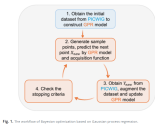
Plasma surface high-order harmonics generation (SHHG) driven by intense laser pulses on plasma targets enables a high-quality extreme ultraviolet (EUV) source with high pulse energy and outstanding spatiotemporal coherence. Optimizing the performance of SHHG is important for its applications in single-shot imaging and EUV absorption spectroscopy. In this work, we demonstrate the optimization of laser-driven SHHG by an improved Bayesian strategy. A traditional Bayesian algorithm is first employed to optimize the SHHG intensity in a two-dimensional parameter space. Then, an improved Bayesian strategy, using the Latin hypercube sampling technique and a dynamic acquisition strategy, is developed to overcome the curse of dimensionality and the risk of local optima in a high-dimensional optimization. The improved Bayesian optimization approach is efficient and robust in convergent to a stable condition in multi-dimensionally optimizing the harmonic ellipticity and intensity. This paves the way for generating a high-quality coherent EUV source with a high repetition rate and promoting further EUV applications.

1741358677131.png
Please, Log in or Register to view URLs content!
 

tphuang

General
Staff member
Super Moderator
VIP Professional
Registered Member

Fuga Gallium Industry has made a breakthrough in gallium oxide MOCVD homoepitaxial technology, helping the downstream vertical power electronic device industry to land​


Hangzhou Fuga Gallium Technology Co., Ltd. (hereinafter referred to as Fuga Gallium), an incubated enterprise of the Hangzhou Institute of Optics and Fine Mechanics, has made important technological breakthroughs in the research and development of gallium oxide MOCVD homoepitaxial thin films. A thin film with a thickness of more than 10 microns was homoepitaxially grown on Fuga Gallium's gallium oxide single crystal substrate. Verified by national authoritative testing agencies, this technology has reached the international leading level. Related standardized products will be launched in April 2025, providing key material support for high-end equipment such as new energy vehicle high-voltage platforms and smart grid flexible transmission devices.

The test results of the third-party testing agency, China National Institute of Metrology, show that the background carrier concentration of the MOCVD epitaxial film is controlled as low as 3.6E15 cm-3, and the mobility reaches 172.7 cm2/V·s. The successful development of high-quality gallium oxide homoepitaxial film based on MOCVD technology will help the rapid implementation of the vertical high-voltage power electronic device industry above 3300V in the future.
View attachment 147244

Fuga Gallium uses MOCVD technology, based on its self-produced gallium oxide substrate products, and through substrate surface optimization, multi-step epitaxial growth and other process strategies, it has greatly improved the crystal quality and thickness of the epitaxial film, and achieved gallium oxide homoepitaxial films with low background carrier concentration and high mobility, and its comprehensive performance indicators have reached the international advanced level . The successful development of MOCVD homoepitaxial films with a thickness of more than 10 microns shows that the MOCVD epitaxial technology route has the ability to mass-produce thick, high-quality gallium oxide homoepitaxial wafers, and can provide material support for the development of vertical gallium oxide power devices.

Please, Log in or Register to view URLs content!
nice, so they've now gotten Gallium Oxide epitaxy to work.

I'm not sure in the future if we are going to use GaO-on-GaO wafers.
 
Top