Chinese semiconductor thread II

tokenanalyst

Brigadier
Registered Member
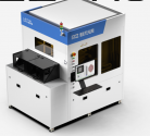
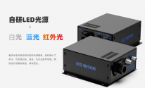
The first 28nm coating precision measuring equipment from Meijie Optoelectronics was successfully installed in Pudong
Please, Log in or Register to view URLs content!
This guys started their business repairing and refurbishing semiconductor equipment, now they even are developing their own inhouse LED powered non contact full field exposure litho machine.

1707766994274.png1707767254025.png
Please, Log in or Register to view URLs content!
 

tokenanalyst

Brigadier
Registered Member

728 million yuan! Yaxiang Integration wins the bid for 12-inch memory base clean room project​

Yaxiang Integration announced that the company recently received a bid winning notice from the Information Industry Electronics Eleventh Design Institute Technology Engineering Co., Ltd. (Project No.: GN2023-06- 8412), confirming that Yaxiang Integration has become the contractor of the clean room system package for the second phase of the 12-inch memory wafer manufacturing base project.
The new project is located in the Airport Economic Demonstration Zone in Hefei City, Anhui Province. The bidding unit is the Information Industry Electronics Eleventh Design Institute Technology Engineering Co., Ltd., and the construction unit is Changxin Xinqiao Storage Technology Co., Ltd. The winning bid amount is 728 million yuan.

According to reports, Changxin Xinqiao Storage Technology Co., Ltd. was established on January 5, 2021, and its registered address is No. 2788 Xinhuai Avenue, Economic and Technological Development Zone, Hefei City, Anhui Province. The business scope includes storage technology services; integrated circuit design, manufacturing, processing, technology development, technology transfer, technology consulting, technical services, technical training and technical testing; electronic product sales and provision of after-sales and technical services; semiconductor integrated circuit chip research and development, Design, entrusted processing and sales; design and development of computer software and hardware and network software and hardware products; sales of computer software and hardware and auxiliary equipment, electronic components and communication equipment; equipment and house leasing; industrial mergers and acquisitions; self-operation and agency of various types Import and export business of goods and technology.

Yaxiang Integration stated that the smooth implementation of this project will help improve the company's business undertaking capabilities, provide more experience for the company's subsequent project development and cooperation, and will have a positive impact on the company's operating performance.
Please, Log in or Register to view URLs content!
 

BoraTas

Captain
Registered Member
N+2 production large enough for 500k to 1 million Ascend chips (I find that hard to believe)
says limitation to Ascend is actually getting HBM3, which is still not domestically produced
I don't. Even at a very pessimistic guess of 35 chips per wafer, 1 million translates to 82 wafers per day. At, again pessimistic, 80 exposures per wafer for the N+2 process, the demand for 1 million Ascends could be satisfied by a single NXT2050i. Of course, they aren't going to use such machines for non-critical layers. HBM3 is a problem indeed. I expect HBM2E from China this year, and HBM3 within 2 years.
 

tphuang

Lieutenant General
Staff member
Super Moderator
VIP Professional
Registered Member
I don't. Even at a very pessimistic guess of 35 chips per wafer, 1 million translates to 82 wafers per day. At, again pessimistic, 80 exposures per wafer for the N+2 process, the demand for 1 million Ascends could be satisfied by a single NXT2050i. Of course, they aren't going to use such machines for non-critical layers. HBM3 is a problem indeed. I expect HBM2E from China this year, and HBM3 within 2 years.
i'm actually estimating around 20 chips per wafer. Beyond Ascend, you need to sell also Kunpeng chips to go with it, which is also quite low yielding. And of course, the biggest demand for Huawei is Kirin chips.
 

BoraTas

Captain
Registered Member
i'm actually estimating around 20 chips per wafer. Beyond Ascend, you need to sell also Kunpeng chips to go with it, which is also quite low yielding. And of course, the biggest demand for Huawei is Kirin chips.
TSMC gets around 65 H100s per wafer. I think 40+ is very realistic for SMIC, even if they have significantly lower yields and Huawei did nothing to compensate for that.
 

tphuang

Lieutenant General
Staff member
Super Moderator
VIP Professional
Registered Member
TSMC gets around 65 H100s per wafer. I think 40+ is very realistic for SMIC, even if they have significantly lower yields and Huawei did nothing to compensate for that.
They need to start doing chiplet. 800mm2 die is hard to get yield up.

I presume that’s the plan for 920.

for all the talk from Huawei people about stacking and advanced packaging, we have not seen much of it yet.
 

BoraTas

Captain
Registered Member
They need to start doing chiplet. 800mm2 die is hard to get yield up.

I presume that’s the plan for 920.

for all the talk from Huawei people about stacking and advanced packaging, we have not seen much of it yet.
Chips designed for embarrassingly parallel workloads like AI have their yields not strongly affected by chip size. Such chips has so much duplication that faults are usually either inconsequential or can be isolated away after testing. In fact, extra size sometimes mean a higher yield if the reason for the added size is sections to improve the yield like redundant logic, fuses to isolate faulty parts etc... They wrote about Cerebras' wafer scale chip on this thread. The production yield for that chip is 100% despite its size of 46225 mm2. For consumer CPUs, it is a different matter. Those chips don't have much independent sections or logic redundancy. Chiplets were also about cutting design costs for AMD, not just for cutting fabbing costs. They generated a lot of CPUs from a few designs. Have you ever wondered why they didn't apply their chiplet expertise to their lowly performing GPU products until the end of 2022? Size simply doesn't matter much for GPU yields.
 

latenlazy

Brigadier
Chips designed for embarrassingly parallel workloads like AI have their yields not strongly affected by chip size. Such chips has so much duplication that faults are usually either inconsequential or can be isolated away after testing. In fact, extra size sometimes mean a higher yield if the reason for the added size is sections to improve the yield like redundant logic, fuses to isolate faulty parts etc... They wrote about Cerebras' wafer scale chip on this thread. The production yield for that chip is 100% despite its size of 46225 mm2. For consumer CPUs, it is a different matter. Those chips don't have much independent sections or logic redundancy. Chiplets were also about cutting design costs for AMD, not just for cutting fabbing costs. They generated a lot of CPUs from a few designs. Have you ever wondered why they didn't apply their chiplet expertise to their lowly performing GPU products until the end of 2022? Size simply doesn't matter much for GPU yields.
This is a very good point. Patterning complexity is a big big determining factor on yield. Something to keep in mind in these discussions.
 
Top