Chinese semiconductor thread II

tokenanalyst

Brigadier
Registered Member

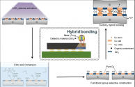
Low-temperature Cu/SiO2 hybrid bonding based on Ar/H2 plasma and citric acid cooperative activation for multi-functional chip integration.​

Abstract​

Cu/SiO2 hybrid bonding is a crucial technique for three-dimensional (3D) integration, which can greatly shorten the interconnected spacing by metal-electrode (Cu) and insulator (SiO2) hybrid interfaces without requiring microbumps. By this bumpless hybrid bonding, the vertical stack of devices with ultrahigh density can be accomplished to meet the demand of high-performance artificial intelligence (AI) chips. To improve the compatibility for multi-functional chip integration, low-temperature bonding conditions are essential. Moreover, it is a great challenge to achieve oxide-free Cu/Cu bonding interface as well as ensure SiO2/SiO2 bonding with sufficient hydroxylated groups. Therefore, we proposed a two-step cooperative activation process as argon and hydrogen gas mixture (Ar/H2) plasma activation followed by citric acid treatment, which makes the Cu oxide reduction and SiO2 hydroxylation simultaneously. The low-cost Cu/SiO2 hybrid bonding was successfully obtained at 200 °C in ambient air. There were nearly neither oxides at Cu/Cu bonding nor residual carbon at SiO2/SiO2 bonding interfaces. More interestingly, the bonding pairs not only survived in the aging tests in the range of 150–350 °C, but the bonding area and strength were further improved. Consequently, this two-step cooperative activation process has great potential for low-temperature Cu/SiO2 hybrid bonding with high-temperature reliability.
1711643222040.png

Please, Log in or Register to view URLs content!
 

tokenanalyst

Brigadier
Registered Member

Dependence of spectral purity of Gd plasma emission around 6.7 nm on laser irradiation conditions​

School of Physics, Changchun University of Science and Technology, Changchun,
Chongqing Research Institute,
Changchun University of Science and Technology,
Zhongshan Institute of Changchun University of Science and Technology,
Shanghai Institute of Optics and Fine Mechanics, Chinese Academy of Sciences,

Abstract​

Gadolinium is a compelling candidate for the next-generation 6.x nanolithography light source. We present a systematically study on the spectral purity at 6.7 nm in the gadolinium laser produced plasma. Variations in extreme ultraviolet spectra are observed over a wide range of laser focal spot sizes and laser pulse energies due to the combined effect of plasma temperature and opacity. When varying laser focal spot size, ionic populations of Gd ions at different electron temperatures were estimated by the collisional-radiative model for the explanation of changes in the spectral profile. When adjusting the laser pulse energy, modifications in the electron density profile were measured through Nomarski interferometry, and the related optical depth was quantified assisted with a one-dimensional radiation transfer model. Results show that, appropriate laser energy and focal spot size are necessary to achieve the high spectral purity, and with a lens with focal length of f = 175 mm and a laser pulse energy of 100 mJ, a spectral purity of Gd plasma up to 3.7% over range of 5.5–10 nm is achieved.

Experimental setup​

The experimental setup of Gd target laser produced plasma source is shown in Fig. 1. Q-switched Nd: YAG laser (Continuum Surelite III) with an 8 ns full-width at half-maximum (FWHM) pulse duration at a wavelength of 1064 nm was used as the driving laser for generating the extreme ultraviolet light source. The laser beam was focused on the target surface. During the experiment, the spot size was adjusted by changing lenses with different focal lengths (f = 400 mm, f = 300 mm, f = 175 mm, and

Result and discussion​

First, the spectra were measured at various lens focal lengths, ranging from f = 100 mm to f = 400 mm, with a fixed laser energy of 100 mJ. The extreme ultraviolet spectra of gadolinium plasma within the range of 5.5–10 nm are depicted in Fig. 2. The observed spectra are dominated by a broad feature peak near 6.7 nm, which is mainly contributed by n = 4-n = 4 unresolvable transition arrays of Gd11+-Gd27+ ions. Region I (6–6.9 nm) of the spectrum is primarily contributed by Gd ions with an open

Conclusions​

In summary, we investigated the spectral purity of laser-produced gadolinium plasma under various irradiation conditions. First, the experimental results with fixed laser energy of 100 mJ and varied lens conditions show that the spectrum of extreme ultraviolet first narrows and then broadens slightly as the focal spot size decreases. Theoretical calculations indicate that migrations of 4d (Gd11+-Gd17+) and 4f (Gd18+-Gd27+) ions are mainly responsible for the changes in the extreme ultraviolet.

Please, Log in or Register to view URLs content!
 

tokenanalyst

Brigadier
Registered Member

Xinlian Integration: In 2024, the company will also plan to build the first 8-inch SiC MOSFET test line in China​


In response to investor questions recently, Xinlian Integration said that the company will invest in the research and development and production capacity construction of SiC MOSFET chips and module packaging technologies from 2021. It has completed three rounds of technology iterations in two years and completed the planar technology for main drives. A breakthrough in SiC MOSFET technology. At present, the performance of the company's latest generation SiC MOSFET products has reached the world's leading level, and SiC MOSFET devices and modules used in vehicle main drive inverters will also be mass-produced in 2023. As of December 2023, the company's 6-inch SiC MOSFET production line has achieved a monthly output of more than 5,000 pieces. In 2024, the company also plans to build the country's first 8-inch SiC MOSFET test line. The company has cooperated with a number of leading car companies and will continue to expand more new energy vehicle OEMs and parts customers in the future. With the advancement of product verification and the continuous improvement of production capacity, the number of SiC MOSFET products on the market will rapidly increase, and operating income will also increase significantly, continuing to consolidate the company's leading position in the field of domestic automotive-grade chip foundry and module packaging and testing.

Please, Log in or Register to view URLs content!
 

measuredingabens

Junior Member
Registered Member
Please, Log in or Register to view URLs content!

High-performance ferroelectric field-effect transistors with ultra-thin indium tin oxide channels for flexible and transparent electronics​

Abstract​

With the development of wearable devices and hafnium-based ferroelectrics (FE), there is an increasing demand for high-performance flexible ferroelectric memories. However, developing ferroelectric memories that simultaneously exhibit good flexibility and significant performance has proven challenging. Here, we developed a high-performance flexible field-effect transistor (FeFET) device with a thermal budget of less than 400 °C by integrating Zr-doped HfO2 (HZO) and ultra-thin indium tin oxide (ITO). The proposed FeFET has a large memory window (MW) of 2.78 V, a high current on/off ratio (ION/IOFF) of over 108, and high endurance up to 2×10⁷ cycles. In addition, the FeFETs under different bending conditions exhibit excellent neuromorphic properties. The device exhibits excellent bending reliability over 5×10⁵ pulse cycles at a bending radius of 5 mm. The efficient integration of hafnium-based ferroelectric materials with promising ultrathin channel materials (ITO) offers unique opportunities to enable high-performance back-end-of-line (BEOL) compatible wearable FeFETs for edge intelligence applications.
 

FairAndUnbiased

Brigadier
Registered Member

Low-temperature Cu/SiO2 hybrid bonding based on Ar/H2 plasma and citric acid cooperative activation for multi-functional chip integration.​

Abstract​

Cu/SiO2 hybrid bonding is a crucial technique for three-dimensional (3D) integration, which can greatly shorten the interconnected spacing by metal-electrode (Cu) and insulator (SiO2) hybrid interfaces without requiring microbumps. By this bumpless hybrid bonding, the vertical stack of devices with ultrahigh density can be accomplished to meet the demand of high-performance artificial intelligence (AI) chips. To improve the compatibility for multi-functional chip integration, low-temperature bonding conditions are essential. Moreover, it is a great challenge to achieve oxide-free Cu/Cu bonding interface as well as ensure SiO2/SiO2 bonding with sufficient hydroxylated groups. Therefore, we proposed a two-step cooperative activation process as argon and hydrogen gas mixture (Ar/H2) plasma activation followed by citric acid treatment, which makes the Cu oxide reduction and SiO2 hydroxylation simultaneously. The low-cost Cu/SiO2 hybrid bonding was successfully obtained at 200 °C in ambient air. There were nearly neither oxides at Cu/Cu bonding nor residual carbon at SiO2/SiO2 bonding interfaces. More interestingly, the bonding pairs not only survived in the aging tests in the range of 150–350 °C, but the bonding area and strength were further improved. Consequently, this two-step cooperative activation process has great potential for low-temperature Cu/SiO2 hybrid bonding with high-temperature reliability.

View attachment 127324

Please, Log in or Register to view URLs content!
Oh hey this looks like some work on cold welding of Au bond pads except with Cu. I remember some experiment of comparing efficacy of bonding and resultant surface energy between using Ar and O2 plasma clean for said bond pads. Surprised they even needed a citric acid clean. For UHV wafer bonding isn't all you need an in situ plasma clean step?
 

mst

Junior Member
Registered Member
Please, Log in or Register to view URLs content!


WASHINGTON, March 28 (Reuters) - The Biden administration is drawing up a list of advanced Chinese chipmaking factories barred from receiving key tools, three people familiar with matter said, to make it easier for companies to stem technology flows into China.
The list could be released in the next few months, one of the people said.
 

latenlazy

Brigadier
Oh hey this looks like some work on cold welding of Au bond pads except with Cu. I remember some experiment of comparing efficacy of bonding and resultant surface energy between using Ar and O2 plasma clean for said bond pads. Surprised they even needed a citric acid clean. For UHV wafer bonding isn't all you need an in situ plasma clean step?
Maybe for residual oxidation? Copper can be like that.
 
Top