You are using an out of date browser. It may not display this or other websites correctly.
You should upgrade or use an alternative browser.
You should upgrade or use an alternative browser.
Chinese semiconductor thread II
- Thread starter vincent
- Start date
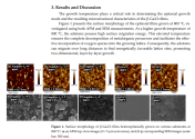
A Pathway to High-Quality Heteroepitaxial Ga2O3 Films via Metalorganic Chemical Vapor Deposition.
Abstract
This work systematically investigates the heteroepitaxial growth of β-Ga2O3 thin films under varied substrate and temperature conditions via metalorganic chemical vapor deposition (MOCVD). Comprehensive characterization reveals that both the substrate type and growth temperature significantly influence the crystalline quality, surface morphology, chemical composition, and defect structure. Films grown at higher temperatures generally exhibit superior crystallinity and closer-to-stoichiometry composition, and thus suggest a reduction in oxygen deficiency. Certain substrates are shown to facilitate high-quality epitaxial growth with smooth surfaces and excellent crystallographic alignment. These findings offer key insights into optimizing growth parameters for high-performance β-Ga2O3-based devices.
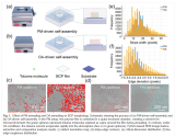
Precision Microenvironment-Driven Isothermal Annealing for the Self-Assembly of Perpendicular Block Copolymers in High-Resolution Lithography Applications.
Abstract:
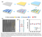
Block copolymer (BCP) nanolithography offers potential beyond traditional photolithographic limits, yet reliably producing low-defect, perpendicular domains remains challenging. We introduce a microenvironment-driven isothermal annealing method for directed self-assembly of BCP thin films. By annealing films at stable temperature in a quasi-sealed, inert-gas chamber, our approach promotes highly uniform perpendicular lamellar nanopatterns over large areas, effectively mitigating environmental fluctuations and emulating solvent-vapor annealing without solvent exposure. Resulting BCP structures demonstrate enhanced spatial coherence and notably low defect density. Furthermore, we successfully transfer these nanopatterns into precise metal nano-line arrays, confirming the method’s capability for high-fidelity pattern replication. This scalable, solvent-free technique provides a robust, reliable route for high-resolution nanopatterning in advanced semiconductor manufacturing.
Baidu Emerging as a Leading AI Chip Player Amid Nvidia Ban
Baidu is rapidly becoming China’s foremost domestic AI chip provider, stepping into the void left by U.S. restrictions that block Nvidia from selling its high-end GPUs to China. Leveraging its subsidiary Kunlun Core, Baidu has developed its Kunlun series of AI chips designed for large language model (LLM) training, inference, cloud computing, and enterprise workloads.
The company, already a leader in AI and autonomous vehicles, is now pursuing a “full-stack” AI strategy integrating its own chips, servers, data centers, and models like Wenxin Yiyan. Baidu’s chip business is gaining traction: it recently secured a major order from China Mobile, and analysts predict explosive growth, with chip sales projected to surge sixfold to 8 billion yuan (~$1.1B) by 2026. Some estimate the Kunlun division could be valued at $28 billion.
Baidu’s five-year roadmap includes launching the Kunlun M100 in 2026 and M300 in 2027, signaling a shift toward full self-reliance. While it still uses a hybrid setup of its own chips and limited Nvidia hardware, the goal is to replace foreign dependencies entirely.
Analysts from Deutsche Bank, JPMorgan, and Macquarie highlight strong domestic demand, government support for local tech, and Baidu’s competitive positioning as key drivers. Though Alibaba and others are also developing AI chips, Baidu is seen as the most advanced and strategically positioned.
Experts agree Baidu’s chip push is both inevitable due to U.S. export controls and highly opportune, as China builds a $10B+ domestic AI hardware ecosystem. If executed successfully, Baidu could become not just a self-sufficient AI player, but a critical infrastructure supplier for China’s entire AI industry.
Seems my google translate cant translate the page.. was their source like cxmt docs?Production Capacity 13% vs Actual Production 6%…The yield gap is 30 to 40 percent
In other words, if the yield of the three memory companies is 90%, CXMT is only 52.2%.
CXMT's HBM yields are extremely low, ranging from 10% to 20%


