Chinese semiconductor thread II

tokenanalyst

Lieutenant General
Registered Member

The Rongke Technology Semiconductor Equipment R&D Project, with a total investment of 1 billion yuan, has commenced construction.​


The R&D and Intelligent Manufacturing Headquarters Project for Key Semiconductor Equipment of Rongke Technology is located east of Yaoxin Road and north of Dongtaihu Road in Hengjing Street, Wuzhong Taihu New City. It has a total investment of 1 billion yuan and covers an area of about 30.27 acres. It is expected to achieve an annual output value of 1.5 billion yuan after reaching full production capacity.

Please, Log in or Register to view URLs content!
 

tokenanalyst

Lieutenant General
Registered Member

Do-Fluoride Chemicals: Current semiconductor-grade hydrofluoric acid production capacity is 40,000 tons/year​

Do-Fluoride Chemicals stated on its interactive platform that the company currently has an annual production capacity of 40,000 tons of semiconductor-grade hydrofluoric acid, and will release capacity according to market demand. The company's lithium hexafluorophosphate production line is currently operating at full capacity, with strong market demand, which is expected to continue its upward trend next year. In terms of demand, the market demand for lithium hexafluorophosphate is highly certain. The company's electronic-grade hydrofluoric acid, electronic-grade silanes, and other electronic chemicals, as well as boron isotope-related products, can meet the needs of high-end semiconductor applications.

Data shows that semiconductor-grade hydrofluoric acid is a high-purity aqueous solution of hydrogen fluoride (HF), and is one of the core wet electronic chemicals in semiconductor manufacturing. The unique characteristic of hydrofluoric acid lies in its selective etching ability towards silicon and silicon oxide (SiO₂)—it can rapidly dissolve SiO₂, but its etching rate towards elemental silicon is extremely low. This characteristic makes it an indispensable key material in semiconductor manufacturing. It is mainly used in core processes such as wafer cleaning, photoresist stripping, etching processes, silicon wafer fabrication, and advanced packaging.

1764602172000.png

Please, Log in or Register to view URLs content!
 

tokenanalyst

Lieutenant General
Registered Member

Qingyi Optoelectronics: The high-precision flat panel display photomask project at its Foshan Nanhai base is about to enter the mass production stage.​


Qingyi Optoelectronics stated on its interactive platform that the company's Foshan Nanhai production base held a production launch ceremony on November 14, 2025. The high-precision flat panel display mask project is about to enter the mass production stage, and the high-end semiconductor mask project is also in full swing preparing for mass production.

The high-precision flat panel display mask base mainly produces 8.6-generation and below high-precision FPD masks, especially filling the gap in domestic AMOLED high-precision masks and meeting the high-definition and flexible display needs of the 5G and AI era; the high-end semiconductor mask base focuses on the production of 180nm-28nm process semiconductor masks. The commissioning of the Foshan Nanhai production base will further expand the company's production scale.

According to public information, Qingyi Optoelectronics is a leading company in China's photomask industry. Founded in August 1997, it was transformed from Qingyi Precision Optoelectronics (Shenzhen) Co., Ltd., and was listed on the Shanghai Stock Exchange's Science and Technology Innovation Board on November 20, 2019. The company primarily engages in the R&D, design, production, and sales of photomasks. Its products are mainly used in flat panel displays, semiconductor chips, touch screens, and circuit boards, with downstream applications covering consumer electronics, automotive electronics, artificial intelligence, and other fields.

Please, Log in or Register to view URLs content!
 

tokenanalyst

Lieutenant General
Registered Member

First Laser's TGV equipment is delivered in batches: a domestic packaging revolution on 1.8mm glass.​

Shoulai Laser has achieved a major industrial breakthrough with the mass delivery of its domestic TGV (Through-Glass Via) equipment, enabling high-precision processing of 1.8mm BF33 glass substrates a critical material for next-generation advanced packaging. Previously dominated by foreign suppliers, this technology has been a global challenge due to the extreme hardness and brittleness of BF33 glass, particularly when drilling micron-scale vias (6μm diameter) with a 10:1 depth-to-diameter ratio.

1764603802931.png

Key Technological Breakthroughs:
  • Ultra-high peak power lasers reduce crack rates to <0.01%.​
  • Innovative laser-chemical step etching achieves ±0.5μm dimensional accuracy and surface roughness Ra≤0.1μm — finer than a dust particle.​
  • Large-format 510×515mm processing system enables simultaneous processing of up to 200 chips, with 3x higher efficiency than imported machines.​
Competitive Advantages Over Imports:
  • Yield: >98% (2% higher than foreign equivalents).​
  • Cost: Unit processing cost reduced to 1/3 of imported equipment — now cheaper than a smartphone per hour.​
  • Delivery: Lead time slashed from 6 months to 45 days, with 24-hour on-site commissioning.​
1.8mm BF33 glass is now the industry benchmark for high-end applications like AI chip HBM stacking and MEMS vacuum packaging offering superior mechanical stability and thermal expansion matching compared to silicon-based TSVs, which suffer from high dielectric loss and thermal mismatch.

Shoulai Laser’s success marks China’s first complete closed-loop innovation in TGV core equipment breaking decades of foreign technological and supply chain dominance. This milestone transforms China’s advanced packaging industry from “import-dependent” to “self-reliant,” accelerating domestic semiconductor development and positioning China as a key player in the global race for next-gen chip packaging.

Please, Log in or Register to view URLs content!
 

swcc

New Member
Registered Member
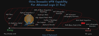
SemiAnalisys, yikes, they are the worst source for this kind of stuff.
SiCarrier Alone Already make most of the stuff in that list, let alone the other players.

View attachment 165490
What about GDDR SDRAMs? any generation, i've searched in this forum and it seems no chinese companies produce them? I've also searched elsewhere. Lisuan's GPU only use GDDR6. They need to make GDDR7, GDDR6, etc. Will cxmt produce them?
 

tphuang

General
Staff member
Super Moderator
VIP Professional
Registered Member
What about GDDR SDRAMs? any generation, i've searched in this forum and it seems no chinese companies produce them? I've also searched elsewhere. Lisuan's GPU only use GDDR6. They need to make GDDR7, GDDR6, etc. Will cxmt produce them?
As a new member on this forum, please understand that this is a heavily moderated thread to keep content quality high and your quality of posts have been pretty low so far. And you have explicitly responded to my post that have bolded red. That is a big no no to do so on this forum.

I would advise you at this point to take a pause from posting here and do a little more reading if you do not want to face further actions.
 

tokenanalyst

Lieutenant General
Registered Member

The 8-inch MEMS wafer production and R&D building of the North Microelectronics Institute has been put into use, propelling the multi-billion-yuan micro-nano manufacturing industry onto the "fast track".​

The North Microelectronics Research Institute (NMRI) officially launched its new 8-inch MEMS wafer production and R&D building, marking a major milestone in China’s micro-nano manufacturing sector. The event coincided with the 46th anniversary of the 214th Research Institute of China Ordnance Industry.

The facility, recognized as China's first fully automated 8-inch MEMS production line, the first mass-production line for piezoelectric materials, and the first flexible electrode line for brain-computer interfaces, signifies a breakthrough in achieving independent control over key sensor chip technologies and breaking foreign technological monopolies.

In his speech, Party Secretary and Chairman Chen Binggen highlighted that this commissioning is a critical step in NMRI’s "6 R&D, 8 Production" strategy, officially putting the billion-yuan micro-nano industry on a “fast track.” He urged staff to uphold high standards, full capacity, and proactive innovation, aiming for key technology breakthroughs, scaled production, and global market expansion.

The launch ceremony was marked by a symbolic cut of a golden road by Chen Binggen and General Manager Xu Chunye, followed by technical personnel entering the cleanroom—signaling the start of operational activities. NMRI aims to transform "possibility" into "feasibility," building an internationally competitive micro-nano manufacturing cluster through solid, down-to-earth efforts.

Affiliated with China North Industries Group, NMRI is a leading integrated microelectronics research and production group in China, covering eight major specialties including MEMS, semiconductors, optoelectronics, advanced packaging, and intelligent sensing. It operates ten domestic process platforms, including the 8-inch MEMS and brain-computer interface lines, and hosts over twenty provincial or national-level innovation centers.

Please, Log in or Register to view URLs content!
 

tokenanalyst

Lieutenant General
Registered Member
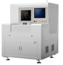
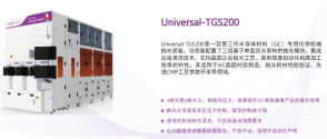
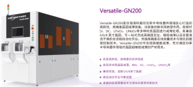
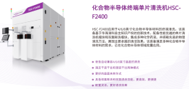
Huahai Qingke Co., Ltd. (hereinafter referred to as "Huahai Qingke") showcased its series of advanced semiconductor equipment and process integration solutions at the 6th Asia-Pacific International Conference on Silicon Carbide and Related Materials. The conference, themed "Connecting the New World with Chips, Inspiring the Future with Intelligence," focused on innovation across the entire wide-bandgap semiconductor industry chain and explored its industrial application prospects in power electronics, new energy, communication technology, and intelligent transportation. Exhibition Highlights: Industry-Leading Technical ExchangeHuahai Qingke Co., Ltd. (688120) showcased its cutting-edge semiconductor equipment and process solutions at the 6th Asia-Pacific International Conference on Silicon Carbide and Related Materials, themed "Connecting the New World with Chips, Inspiring the Future with Intelligence."

Highlighting industry leadership, Huahai Qingke attracted wide attention with three key high-end products:​
  • Universal-TGS200: Advanced CMP equipment for third-generation semiconductors, enabling precise surface planarization.​
  • Versatile-GN200: High-rigidity, ultra-precision wafer thinning machine ensuring yield and reliability.​
  • HSC-F2400: High-efficiency single-wafer cleaning system that guarantees device performance through superior cleanliness.​
1764623547183.png
1764623616364.png
1764623681524.png


These solutions form a complete compound semiconductor manufacturing platform, supporting domestic high-end equipment development.

Building on its "equipment + service" strategy, Huahai Qingke offers a broad product range in CMP, ion implantation, thinning, scribing, edge polishing, and wet processing, backed by comprehensive services like wafer regeneration and consumable maintenance. The solutions are widely applied in ICs, advanced packaging, large wafers, SiC semiconductors, and MEMS.

Committed to self-reliance and innovation, the company has made significant R&D advances in core semiconductor equipment. Looking ahead, Huahai Qingke will continue developing next-generation equipment and integrated solutions to drive high-quality industrial growth.

Please, Log in or Register to view URLs content!
 
Top