
You are using an out of date browser. It may not display this or other websites correctly.
You should upgrade or use an alternative browser.
You should upgrade or use an alternative browser.
Strategic implications of Chinese/US AI development
- Thread starter shifty_ginosaji
- Start date
Hendrik_2000
Lieutenant General
nop, 7nm u need better mask and optics
china right now can do 22nm which is half a decade behind.
machines come from europe/america
Well I am not expert in semiconductor but the article clearly said there is way to make 10nm using the new technology by double patterning
the maximum line width resolution of a single exposure reached 22 nanometers (about 1 / 17 exposure wavelength). On this basis, the project team also combined the high-aspect ratio etching and multi-patterning technology developed by the super-resolution lithography equipment project to realize the processing of feature size graphics below 10 nm.
antiterror13
Brigadier
Well I am not expert in semiconductor but the article clearly said there is way to make 10nm using the new technology by double patterning
Wondering, apart from TSMC, Intel, Samsung and GF .. is there any other companies that currently is able to manufacture better than 22nm ?
Is there any military hardware chips with 22nm technology or better?
Combat hardware typically uses lower generation processes which have lower transistor failure rates in higher radiation environments.
You might see the higher density chips be used in things like supercomputers used to design and test equipment or conduct R&D. Or in leading consumer mobile computing productions.
You might see the higher density chips be used in things like supercomputers used to design and test equipment or conduct R&D. Or in leading consumer mobile computing productions.
The semi industry is in a coffin corner for six years now.EUV will not be economic for at least a couple of years. Nearly every process over the last decade has involved ArF (193 nm) light sources. Later water immersion and multiple patterning were used to increase feature detail at the expense of system complexity and, with patterning, of wafer output. The industry was supposed to develop CaF2 (157 nm) light sources as a replacement for ArF at the start of this century. But those never entered production, because of difficulties with the technology, they decided to "leap ahead" to EUV and the industry has been stuck on EUV (13.5 nm) light source R&D for like two decades with little progress made in that time period. I think the Japanese manufacturers of lithography tools were among the last to give up on CaF2 light source research. Had that been persisted with we probably could have been making chips with more wafer output right now.
Because they cannot use lower wavelength light sources the industry has had to play with diffraction masks and multiple patterning. But if you use double-patterning, for example, you halve the amount of wafers output per day. This means your factory's production is cut in half. Today it is common to use quadruple-patterning and more. Further reducing wafer output.
At 130 nm the frequency increase stopped around 2002.
In 2012 with the 22nm technology the industry reached the maximum number of simultaneously working transistors .
The 28nm technology was the minimum cost point for semiconductors, due to the exploding cost of masks / machines/clean room and so on.
The EUV can not make faster ICs , all that it can achieve is to run smaller batches- maybe, but considering that the validation cost on the new nodes exploding as well it is doubtful.
The talk about AI is nothing else just how to get out more from the available 1 billion/sqcm transistor, on 3GHz.
It is pathetic, goes back to the age of analogue computers.
And it can not generate the same strategic advantage that the semi industry gave to the USA during the 70s/80s/90s.
The mass / cost difference of the same computing capacity was one-two magnitude for the advance of the USA that time, but even the most cutting edge AI can give only % difference.
Hendrik_2000
Lieutenant General
Vincent just posted the underlying science behind the new lithograph machine. I just posted excerpt from the paper Anyone interested can click on the link
Here is a paper about surface plasmon polaritons
Jianjie Dong1, Juan Liu1, Guoguo Kang1, Jinghui Xie1 & Yongtian Wang1
Scientific Reports volume 4, Article number: 5618 (2014)
Abstract
A deep ultraviolet plasmonic structure is designed and a surface plasmon interference lithography method using the structure is proposed to generate large-area periodic nanopatterns. By exciting the anti-symmetric coupled surface plasmon polaritons in the structure, ultrahigh resolution periodic patterns can be formed in a photoresist. The resolution of the generated patterns can be tuned by changing the refractive index and thickness of the photoresist. We demonstrate numerically that one-dimensional and two-dimensional patterns with a half-pitch resolution of 14.6 nm can be generated in a 25 nm-thick photoresist by using the structure under 193 nm illumination. Furthermore, the half-pitch resolution of the generated patterns can be down to 13 nm if high refractive index photoresists are used. Our findings open up an avenue to push the half-pitch resolution of photolithography towards 10 nm.
Introduction
Optical lithography is the most widely used technique for fabricating large-area integrated devices. However, the resolution of conventional photolithography techniques is limited by the diffraction of light, which makes it difficult for them to meet the demand of fabricating ultrahigh density integrated devices. To overcome this problem, surface plasmon polaritons (SPPs) have been used for lithography. The superlens imaging lithography1,2,3,4,5,6,7, which uses SPPs to amplify evanescent waves to achieve a sub-diffraction-limit resolution, is a promising plasmonic lithography technique. Although this technique has a higher resolution than conventional photolithography techniques, it still faces some obstacles such as the difficulty of fabricating ultrahigh resolution masks. Recently, a superlens system8 used for lithography was proposed to reduce the difficulty in the fabrication of masks by demagnification imaging, but its complex structure leads to an engineering challenge.
The focused plasmon beam lithography9, which uses a focused plasmon beam generated from a plasmonic lens to generate patterns, is a maskless plasmonic lithography technique and hence completely solve the problems involved with masks. By optimizing the structure of the plasmonic lens, its resolution has been improved to 22 nm10. However, it becomes difficult to further improve the resolution of this technique due to the facts that the focused spot size of a plasmonic lens increases with increasing its focal depth and the decay of SPPs increases with reducing their wavelengths.
The surface plasmon interference lithography11,12,13,14,15,16,17,18,19, which can employ the interference effect of SPPs to generate sub-diffraction-limit patterns, which is due to the fact that SPPs have a larger wave vector than light waves of the same frequency11,12, is perhaps the most promising plasmonic lithography technique for fabricating large-area periodic structures such as an array of nanoparticles20,21, an array of nanoholes22,23, and an array of nanowires24,25,26. Since dielectric-metal multilayer structures support ultra-short wavelength SPPs, the surface plasmon interference lithography method (SPILM) using an 8 pairs of GaN and Al multilayer becomes the highest-resolution SPILM among previous SPILMs15. This SPILM can produce 16.5 nm half-pitch one-dimensional (1D) patterns with an image contrast of about 0.2 under 193 nm illumination. However, because the image contrasts of the higher-resolution patterns produced by this SPILM are below 0.2, which don't satisfy the minimum requirement for photoresists, its resolution can't be further improved. It is imperative to overcome the fundamental limitations on the resolution of previous plasmonic lithography techniques for obtaining a higher resolution.
In this paper, a deep ultraviolet plasmonic structure is designed and a SPILM using this structure is proposed to produce ultrahigh resolution patterns with a sufficient image contrast for photoresists. Because the designed structure supports anti-symmetric coupled SPPs with ultra-short wavelengths, the half-pitch resolution of the produced patterns can go beyond 15 nm. Although the proposed SPILM needs a mask, the pitch resolution of the mask is at least two times lower than that of the produced patterns, which can reduce the fabrication difficulty of masks.
Results and Discussion
A schematic of the deep ultraviolet plasmonic structure is shown in Figure 1. This structure consists of an Al grating, an Al2O3 spacer layer, and two Al films separated by a photoresist (PR) layer. The Al grating is located at the bottom surface of a SiO2 substrate, and its openings are filled with Al2O3. The Al2O3 spacer layer is sandwiched between the Al grating and the upper Al film. The lower Al film is coated on a Si substrate. The thicknesses of the Al grating, the Al2O3 spacer layer, the upper Al film, the PR layer and the lower Al film are denoted by d1, d2, d3, d4 and d5, respectively. Al is chosen as the metal material of the plasmonic structure because its dielectric constant has a highly negative real part and its absorption is low in the deep ultraviolet band, which are beneficial to exciting SPPs.
The Al grating is used as a mask. We use a one-dimensional (1D) grating mask to illustrate the principle of the proposed SPILM. A two-dimensional (2D) grating mask can be considered as a combination of two 1D grating masks. We assume that the openings of the 1D grating extend in the z direction. The period and opening width of the 1D grating are denoted by Px and wx, respectively. The PR layer and the two Al films form a plasmonic waveguide. The dispersion relations of the coupled SPPs whose propagation directions are perpendicular to the yz plane in the plasmonic waveguide are given by
Hendrik_2000
Lieutenant General
Via Taishang
China surpasses South Korea to become largest chip equipment market
By Zhang Hongpei Source:Global Times Published: 2018/12/6
Nation hikes investment to cut foreign reliance, while global firms cut back: analysts
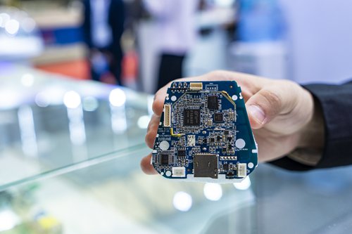
An employee showcases a semiconductor integrated circuit at an industry expo on October 31. Photo: VCG
China has become the world's largest semiconductor equipment market thanks to continuous, intensive investment in the sector.
Although the domestic semiconductor equipment market is forecast to maintain rapid growth in the next two or three years, the investment model should become rational, as money needs to be combined more with technology accumulation and talent cultivation, analysts warned.
The global semiconductor industry association SEMI said in a report that South Korea, which topped the ranking for six quarters, yielded to China. Semiconductor equipment shipment in South Korea stood at $3.45 billion in the third quarter, down 31 percent year-on-year, the first drop since the first quarter of 2016, according to the SEMI.
Meanwhile, China became the largest semiconductor equipment buyer with billings of $3.98 billion, up 106 percent.
In the third quarter of 2017, the figure was just $1.93 billion, about 40 percent of the South Korean total.
The SEMI estimates that equipment sales in China will surge 46.6 percent to $17.3 billion in 2019.
"China's first ranking is more related to South Korea's slower pace of increase than the continuous equipment investment in China," Han Xiaomin, general manager of CCID Consulting's integrated circuit business, told the Global Times on Thursday.
Given sluggish demand in overseas markets that has persisted since last year, some international semiconductor giants have been cutting their investment in equipment. They may be seeking changes in their technology direction as well, Han said.
In comparison, the Chinese market has experienced booming development with ramped-up efforts from the government and companies to grow the chip sector.
In 2014, Beijing established the China Integrated Circuit Industry Investment Fund, also known as the "Big Fund," with support from the
and other entities. The fund's aim is to help build a competitive chip ecosystem for China so that the country can cut its heavy reliance on foreign suppliers.
The first-phase fund completed investment of 138.7 billion yuan ($20.12 billion) in total in May, media reports said.
Meanwhile, more Chinese companies have been showing an interest in the IC sector, especially this year. For example, e-commerce company Alibaba Group Holding unveiled in September an ambitious plan to develop a proprietary artificial intelligence (AI) chipset, and it said it will establish a semiconductor company, named Pingtouge, to meet this goal.
Semiconductor equipment plays a vital role in the manufacturing of ICs, standing at the upstream of the semiconductor industrial chain. "About 70 percent of investment in the industry goes into equipment, which is used to manufacture and test chips," Han said.
Wang Yanhui, head of the Shanghai-based Mobile China Alliance, told the Global Times on Thursday that semiconductor equipment, which requires advanced technology and long-term research and development as well as skilled technicians, is not where China has absolute advantages. Thus most of this equipment is imported, even though in some niche markets, domestically produced equipment can equal or even surpass imported items.
"Traditional powerhouses such as the US, the Netherlands and Japan still dominate the upstream of the semiconductor industrial chain, while China's advantages cluster in chip manufacturing, which is at the downstream of the chain," said Wang.
Analysts said that industry logic dictates a reliance on a connected global market and international division of labor.
"You cannot expect one nation to handle the whole industrial chain," Wang noted.
He added that as China is constantly investing in equipment, it must keep an eye on the connection of that investment with technological improvement and talent training.
"China's IC industry can follow the smartphone development path -
from knock-offs to core technology development and own-brand products," he added.
China surpasses South Korea to become largest chip equipment market
By Zhang Hongpei Source:Global Times Published: 2018/12/6
Nation hikes investment to cut foreign reliance, while global firms cut back: analysts
An employee showcases a semiconductor integrated circuit at an industry expo on October 31. Photo: VCG
China has become the world's largest semiconductor equipment market thanks to continuous, intensive investment in the sector.
Although the domestic semiconductor equipment market is forecast to maintain rapid growth in the next two or three years, the investment model should become rational, as money needs to be combined more with technology accumulation and talent cultivation, analysts warned.
The global semiconductor industry association SEMI said in a report that South Korea, which topped the ranking for six quarters, yielded to China. Semiconductor equipment shipment in South Korea stood at $3.45 billion in the third quarter, down 31 percent year-on-year, the first drop since the first quarter of 2016, according to the SEMI.
Meanwhile, China became the largest semiconductor equipment buyer with billings of $3.98 billion, up 106 percent.
In the third quarter of 2017, the figure was just $1.93 billion, about 40 percent of the South Korean total.
The SEMI estimates that equipment sales in China will surge 46.6 percent to $17.3 billion in 2019.
"China's first ranking is more related to South Korea's slower pace of increase than the continuous equipment investment in China," Han Xiaomin, general manager of CCID Consulting's integrated circuit business, told the Global Times on Thursday.
Given sluggish demand in overseas markets that has persisted since last year, some international semiconductor giants have been cutting their investment in equipment. They may be seeking changes in their technology direction as well, Han said.
In comparison, the Chinese market has experienced booming development with ramped-up efforts from the government and companies to grow the chip sector.
In 2014, Beijing established the China Integrated Circuit Industry Investment Fund, also known as the "Big Fund," with support from the
and other entities. The fund's aim is to help build a competitive chip ecosystem for China so that the country can cut its heavy reliance on foreign suppliers.
The first-phase fund completed investment of 138.7 billion yuan ($20.12 billion) in total in May, media reports said.
Meanwhile, more Chinese companies have been showing an interest in the IC sector, especially this year. For example, e-commerce company Alibaba Group Holding unveiled in September an ambitious plan to develop a proprietary artificial intelligence (AI) chipset, and it said it will establish a semiconductor company, named Pingtouge, to meet this goal.
Semiconductor equipment plays a vital role in the manufacturing of ICs, standing at the upstream of the semiconductor industrial chain. "About 70 percent of investment in the industry goes into equipment, which is used to manufacture and test chips," Han said.
Wang Yanhui, head of the Shanghai-based Mobile China Alliance, told the Global Times on Thursday that semiconductor equipment, which requires advanced technology and long-term research and development as well as skilled technicians, is not where China has absolute advantages. Thus most of this equipment is imported, even though in some niche markets, domestically produced equipment can equal or even surpass imported items.
"Traditional powerhouses such as the US, the Netherlands and Japan still dominate the upstream of the semiconductor industrial chain, while China's advantages cluster in chip manufacturing, which is at the downstream of the chain," said Wang.
Analysts said that industry logic dictates a reliance on a connected global market and international division of labor.
"You cannot expect one nation to handle the whole industrial chain," Wang noted.
He added that as China is constantly investing in equipment, it must keep an eye on the connection of that investment with technological improvement and talent training.
"China's IC industry can follow the smartphone development path -
from knock-offs to core technology development and own-brand products," he added.
Hendrik_2000
Lieutenant General
Via Emperor
Here is China chance to pass over the current leader is Semiconductor technology the slowing down of ever increasing density of the chips and new technology like Quantum chips and A1 will give China level playing filed if not lead in these technology. Nothing stay the same ever!
The chips are down
The semiconductor industry and the power of globalisation
Superpower politics may start to unravel it
Print edition | Briefing
Dec 1st 2018 | HONG KONG
Silicon valley, the heartland of America’s technology industry, takes its name from the chemical element that is the most important ingredient in microchips. Most of the attention it now attracts is directed at companies such as Facebook, Google and Apple, which are better known for their software and nifty devices rather than the chips that make them work. But it was in the Valley in the 1950s and 1960s where inventions like the transistor and the integrated circuit were refined, helping to transform computers from unreliable machines the size of a room into dependable devices that fit neatly into pockets. That in turn enabled the technology titans of today to prosper.
Modern microchips are now embedded into everything from cars and washing machines to fighter planes. World Semiconductor Trade Statistics, a data provider, reckons that the market for chips was worth $412bn in 2017, a rise of 21.6% on the year before. If anything, these raw numbers understate the importance of chipmaking. The global e-commerce industry, for instance, is reckoned to have revenues of over $2trn a year. If data are the new oil, chips are the internal-combustion engines that turn them into something useful.
The ubiquity of chips has led to the growth of a vast global industry. Modern microchips have billions of components and are made in ultra-advanced factories that cost tens of billions of dollars to build. Indeed, that such devices can be built at all is a testament to the power of specialisation and trade.
These hugely complicated products have spawned an equally complex supply chain involving thousands of specialised companies all around the world. The Semiconductor Industry Association, an American trade body, reckons that one of its members has more than 16,000 suppliers, of which more than 8,500 are outside the United States. The raw materials and the parts that are the components of a chip cross and recross the world before eventually ending up as the brains of a smartphone, a car’s anti-lock braking system or thousands of other products besides.
Two forces are now thrusting the semiconductor industry firmly into the spotlight. The first is geopolitics. Chips are caught up in an increasingly bad-tempered rivalry between America, the incumbent techno-superpower, and China, the aspiring one. The second is physics. This brewing technological struggle comes at a historic moment. For 50 years progress has been driven by Moore’s law, which states that the number of components that can be crammed onto a chip doubles every two years and thus, roughly, so does its computational power. But the law is breaking down, leaving the future of the industry looking messier and less certain than at any time in the past.
Electronic politics
Start with geopolitics. America has long seen its lead in chipmaking as a vital strategic asset. One of the earliest uses for the chips coming out of Silicon Valley, which owes its existence to the patronage of the Pentagon as much as it does to venture capitalists, was in guidance systems for nuclear missiles. A White House report published in 2017 does not mince its words: “Cutting-edge semiconductor technology is…critical to defence systems and us military strength.”
China also sees chips as crucial to its future. In 2014 it established the National Integrated Circuit Industry Investment Fund, to channel cash to research and development in the semiconductor industry. One of the targets of “Made in China 2025”, a national programme designed to boost high-tech industries, is to increase domestic production. China wants the revenues of its home-grown chip industry to grow from $65bn in 2016 to $305bn by 2030, and for most of its demand for chips to be supplied domestically (today only around a third is).
America has not welcomed China’s incursion onto its patch. It has reacted by trying to slow its rival’s progress. In 2015, for instance, it banned the sale of high-end chips made by Intel, the world’s second-biggest semiconductor firm, to Chinese labs that design supercomputers. It has thwarted acquisitions of American companies by Chinese firms.
This year the Trump administration briefly banned American firms from selling components to zte, a Chinese maker of smartphones and telecoms equipment, after it breached the terms of a settlement to do with illegally exporting technology to Iran. zte has revenues of $16bn and sells its products all over the world. But the Chinese company licenses its chip designs from several American firms and, when that supply was cut off, it was paralysed overnight. Bankruptcy was only averted when Donald Trump, America’s president, unexpectedly agreed to lift the ban.
Chips in the windscreen
America has also levelled allegations of industrial espionage at China. On November 1st prosecutors indicted Fujian Jinhua Integrated Circuit, a Chinese chipmaker, and United Microelectronics Corporation, its Taiwanese partner, accusing them of stealing trade secrets from Micron, a big American firm. Officials have kept up a drumbeat of warnings about the risks of using equipment made in China, for fear that it may be funnelling sensitive information homeward. On October 12th two senators publicly warned Canada not to let Huawei, a big Chinese electronics firm, become involved in plans to build speedy 5g mobile-phone networks in the country. This week, New Zealand blocked a mobile-network operator, Spark, from using Huawei’s equipment in its forthcoming 5g network. And chips are a front in Mr Trump’s tariff-led trade war with China. They are among a range of goods on which America raised duties in August.
China has toughened up in retaliation. A planned takeover by Qualcomm, an American firm that designs chips, of nxp, a Dutch one, was abandoned in 2018 after heel-dragging by competition regulators in Beijing. Chinese authorities are also investigating price-fixing among American and South Korean manufacturers of memory chips, including Micron.
America’s efforts to frustrate China may only serve to make it more determined. Until recently China boasted the world’s fastest supercomputer. Named “TaihuLight”, and based at the National Supercomputing Centre in Wuxi, near Shanghai, its 40,960 ShenWei 26010 chips are of an entirely Chinese design, says Jack Dongarra, a supercomputing specialist at the University of Tennessee. The main result of the Intel ban, he says, is “that China has put even more money into high-performance computing research”. Successor machines to the TaihuLight, using more advanced chips, are in the works.
A trade war and the growing sense of an unfriendly rivalry between America and China is having unwelcome repercussions on one of the world’s most complex and globalised industries. “These [chip] companies have been told that globalisation is great for the past 30 years,” says Paul Triolo of the Eurasia Group, a political-risk consultancy. “And now all of a sudden this has become a national-security problem, and they have to try to adjust to that.”
Refashioning an industry that is vast, fast-growing and vital to the global economy will not be easy. In the early days chipmakers handled every part of the process in-house. That began to change in 1961 when Fairchild Semiconductor began assembling and testing products in Hong Kong, where skilled labour was cheap. That trend has accelerated as chips have become more complicated and more of the manufacturing process has been outsourced to specialised firms. The result is a confusing constellation of thousands of companies. These can be lumped into three rough categories (see diagram)—design, manufacture, and assembly and packaging.
A typical journey from raw silicon to completed chip gives an indication of how elaborate supply chains can be. It may start in the Appalachian mountains, where deposits of silicon dioxide are of the highest quality. The sand may then be shipped to Japan to be turned into pure ingots of silicon. These are then sliced into standard-sized wafers, 300mm across, and sent to a chip factory, or “fab”, perhaps in Taiwan or South Korea. Here the slices will be imprinted with a particular pattern using photolithography equipment made in the Netherlands.
Hendrik_2000
Lieutenant General
(cont)
That pattern will be determined by the overall design of the chip. This design might come from arm, a company based in Britain. But it can be tweaked for specific applications by one of the company’s many licensees. Once finished, it must be assembled into a package, in which the etched silicon is placed inside the familiar ceramic or plastic containers that are dotted across any circuit board, and then comes testing. That might take place in China, Vietnam or the Philippines.
Slices both ways
This is then integrated into a circuit board, which could happen somewhere else again. The result will be one of the many components that arrive at factories from Mexico to Germany to China, for assembly into an industrial robot, smart electricity meter or one of the millions of computers that crunch data in the cloud.
China’s domestic industry started at the lower-value end of this process, says Jiang Xu, a professor of electrical engineering at the Hong Kong University of Science and Technology. Its strength still lies in assembly and packaging chips. Dozens of firms around the Yangzi delta near Shanghai, for instance, specialise in this sort of work. Their names may be unfamiliar—jcet, Tianshui Huatian and tfme—but their revenues are counted in billions of dollars.
Now, with Western firms reliant on it for this work, and fuelled by a fast-growing home market, China is turning to design and manufacturing. It has already made inroads at the lower end of the market. Firms such as Samsung, Intel, Apple and Taiwan Semiconductor Manufacturing Company (tsmc) design or make powerful, expensive chips for smartphones or cloud computing. But “between 75% and 80% of semiconductors are not bleeding-edge products,” says Len Jelinek of ihs Markit, a research firm. Chips that go into lcd televisions, home routers and smart devices that make up the internet of things, which adds sensors and internet connections to everyday objects, “can absolutely be manufactured by firms in China”.
Chinese firms are beginning to succeed further up the value chain, too. HiSilicon (owned by Huawei) and Tsinghua Unigroup, a state-owned firm, are rated among the world’s top ten chip-design firms by revenue. HiSilicon’s “Kirin” series of smartphone chips is on a par with anything Western companies can design.
No Moore
Through these efforts China has reduced dependence on foreign expertise, but not yet eliminated it. Mr Xu points out that Chinese firms still rely heavily on modifying designs from arm. Its chips already dominate the mobile-computing business and are poised to do the same with the array of smart devices that will make up the internet of things. The firm is also trying to break into the market for high-powered cloud-computing chips. Yet arm is based in Britain, and was recently bought by SoftBank, a big Japanese firm. Both are close allies of America.
China has found it harder to make progress in cutting-edge manufacturing, which is the most demanding part of chipmaking. Chinese upstarts must compete with incumbents that have intimidating technological leads and engineers with decades of hard-won know-how. “The semiconductor [manufacturing] industry is really about repetitive cycles of learning,” says Mr Jelinek. The Kirin 980 was the first smartphone chip to be produced on the 7-nanometre node—the current state of the art for squeezing in computing power. Since no fab in China has the required technology, HiSilicon—like Apple and Qualcomm, its American competitors—had to have its chips made in Taiwan, by tsmc.
The demise of Moore’s law could offer a means to restrict China’s ambitions. It has always been clear that it cannot go on indefinitely. Each time components in a chip shrink, manufacturing gets fiddlier and more expensive. Leading-edge fabs have become eye-wateringly pricey. Samsung is spending $14bn to build one near Pyeongtaek, in South Korea. Chipmakers jokingly refer to Moore’s second law, which says that the cost of a chip factory doubles every four years.
The result has been consolidation at the forefront of chipmaking. In 2001 there were 29 companies offering the most advanced fab facilities, according to McKinsey, a consulting firm (see chart). Today there are five. That could make it easier for Western techno-hawks to slow China’s progress. These fabs are owned by companies based in America, or in Taiwan and South Korea, both of which are its allies. Another lever might be the firms that supply equipment to those fabs. One in particular—asml, a Dutch firm—has, after over a decade of trying, finally commercialised “extreme ultra-violet lithography”, a manufacturing process needed for the most advanced chips. That could offer Western policymakers a pinch-point.
But the end of Moore’s law offers China hope, too. One of its side-effects used to be that, as components shrank, chips were able to operate faster. But that effect—called Dennard scaling—broke down in the mid-2000s, which meant that shrinking a chip’s components offered fewer benefits than it used to. For that reason, says Linley Gwennap, a chip-industry analyst, being a pace or two behind the leaders in manufacturing matters a bit less than before.
At the same time, says Andrew Huang, a hardware designer, the slowing of Moore’s law has left the industry as a whole casting about for other ways to build better chips. Attention is gradually shifting, in other words, from refining manufacturing towards cleverer design and new ideas. If that changes the way the chip industry operates, Chinese firms could try to move into this new, relatively unclaimed territory.
HiSilicon’s chips offer an example. They include super-specialised silicon designed to speed up calculations that are useful for artificial intelligence, another focus of “Made in China” and an area into which the country is ploughing cash. Quantum computing is another promising avenue. It uses the effects of quantum mechanics to speed up enormously some sorts of calculations. China has made big bets on quantum computing, reportedly spending $10bn to build a big research lab in Hefei, the capital of Anhui province. But it will require the mastery of unconventional physics such as superconducting wires and ion traps, technologies that are very different from what chipmakers use today.
As China advances at the boundaries of chipmaking, America is trying to push them further out of reach. American firms, including Google, Microsoft and ibm, have quantum-computing projects of their own. A report in 2017 from the President’s Council of Advisors on Science and Technology advised that America’s best response to China’s rise would be to invest to maintain its technological lead. With that in mind darpa, an American military research agency, is running a project called the Electronics Resurgence Initiative (eri), which aims to develop new technologies to the point where they can be commercialised by private firms.
Picking up the pace
Some of its projects are tweaks that aim to improve existing processes. One example, says William Chappell, who runs the eri, is technology to allow small chip-design firms to integrate more easily their specialised silicon into bigger designs from larger companies, which should help cut costs. But eriis also investing in more speculative areas. It has projects looking into optical computing, which aims to build chips that run on light rather than electricity; spintronic transistors, which rely on quantum effects to function; and approximate computing, which sacrifices precision in calculations to save energy.
Making chips even more high-tech could keep America in the driving seat. In any case, says Mr Triolo, it may prove easier than trying to unwind the industry’s global supply chains. Indeed, freezing out China is not something welcomed everywhere in America. Qualcomm, for instance, derives two-thirds of its revenue from China; for Micron the figure is 57%. And a trend towards collaboration, with the likes of Microsoft and Amazon opening research centres in China, has kept investment flowing both ways across the Pacific. A turn to protectionism to keep China in check would inflict damage far beyond its borders.
This article appeared in the Briefing section of the print edition under the headline "The chips are down"