For the continuation of the AI discussion in the Trade War with China thread.

You are using an out of date browser. It may not display this or other websites correctly.
You should upgrade or use an alternative browser.
You should upgrade or use an alternative browser.
Strategic implications of Chinese/US AI development
- Thread starter shifty_ginosaji
- Start date
Hendrik_2000
Lieutenant General
Via emperor. the company is China based subsidiary of Soft bank a separate entity form Soft bank that own the licence on RISC architecture. In order to avoid any arm twisting from you know who
Now some people say china is not doing anything on basic science of Chip making wrong!
This is exactly what China needs. Any microchip firm with good technologies in China will have a solid future due to assured market access and scramble by manufacturers to replace unreliable and very risky RH products.
NOVEMBER 13, 2018 / 6:57 PM / UPDATED 2 HOURS AGO
ARM Holdings to invest $1.4 billion-plus on Sichuan project: Xinhua
1 MIN READ
BEIJING (Reuters) - Chip design company ARM Holdings’ Chinese subsidiary has signed an agreement with southwestern Sichuan province for a more than 10 billion yuan ($1.4 billion) research and development project, the official Xinhua news agency reported on Tuesday.
ARM, owned by Japan’s Softbank Group, will build a new complex on a site of about 200,000 square meters for microchip research and development, the report said.
($1 = 6.9576 Chinese yuan renminbi)
This is kind of odd because ARM mostly designs chips and sells IP licenses. They do not manufacture chips themselves. But it might make sense for them to make an R&D center to develop Chinese market specific chip designs for example. There are not a lot of clients for ARM servers right now and with the issues China has with X86 CPU licenses it might make sense to invest on something like that specifically in China especially if it has government funds attached to it.
Hendrik_2000
Lieutenant General
Well Bloomberg think this will scuttle Chinese ambitions but I see it as blessing in disguise from now on the Chinese cannot expect any help from the west and only spur them to developed domestic technology
The chip maker caught in US assault on China’s tech ambitions
Fujian Jinhua Integrated Circuit Co’s plan to start full-scale production at its US$6 billion plant is now in tatters after the US slammed the door on the firm’s purchase of chip manufacturing equipment
PUBLISHED : Monday, 26 November, 2018, 8:03pm
UPDATED : Monday, 26 November, 2018, 8:19pm
Bloomberg
For a sense of the damage Donald Trump can inflict on China with export controls, take a trip to the city of Jinjiang on the country’s southeastern coast.
That is where Fujian Jinhua Integrated Circuit Co built a US$6 billion plant to produce semiconductors as part of China’s goal of making the country a self-sufficient technology powerhouse. But after the US President barred exports to the company, its dream is now in tatters with consultants from American suppliers gone, the factories silent and workers rattled.
Less than a month ago, Jinhua was full-speed ahead on an enormous undertaking financed by the local government that blanketed its corner of the city with bristling power plants hulking workers’ dormitories and modern research labs. It was within months of a deadline to kick off full-scale production of some 60,000 wafers a month, a key step to giving China a competitive producer of memory chips used in smartphones.
Then the US Justice Department accused it of stealing American technology, and the Department of Commerce slammed the door on purchases of the chip manufacturing gear it needed to hit that milestone. Expansion work halted as its American and even European suppliers skipped town. Now, uncertainty shrouds a company President Xi Jinping has touted as one of three future domestic champions of chip production.
“No one here knows for sure what’s next, not even the local government officials,” one engineer told Bloomberg News on condition of anonymity. “Only Xi Jinping and Donald Trump can save us now. We only hope the government sees us as important as ZTE.”
While the Trump administration can reverse course – as it did with a similar moratorium on ZTE Corp – the case illustrates the ease with which Washington can derail China’s efforts. That may strengthen the mainland’s resolve to build its own chip capabilities so it can – once and for all – shake off a reliance on US$200 billion of annual imports.
Before the indictment, Jinhua was just getting going. In a little over two years, the company amassed a staff of about 1,000 and put together a pilot assembly line cranking out 5,000 (usable) 12-inch wafers a month, enough for millions of chips.
Taiwan’s United Microelectronics Corp (UMC) – once one of the semiconductor industry’s foremost contract producers – was Jinhua’s research and development partner for dynamic random-access memory technology under a licensing agreement.
White-frocked engineers from photolithography systems supplier ASML Holding and US-based chip process control systems provider KLA-Tencor Corp busied themselves on the workshop floor, advising their Chinese clients on the use of their equipment.
The day the US announced its ban, semiconductor manufacturing equipment company Applied Materials staff packed up and left, according to people familiar with the matter. The American company had shipped components to Jinhua as recently as September 20, according to an airway bill seen by Bloomberg.
KLA-Tencor and chip processing equipment provider Lam Research Corp also recalled their engineers, the people said. Even Dutch giant ASML – whose extreme ultraviolet lithography machines are the linchpin in next-generation chip manufacturing – pulled out within days, abandoning work on a second assembly line.
The once-smooth influx of equipment ground to a halt. On a windy afternoon in November, a giant plot of land adjoining Jinhua’s campus earmarked for its second facility stood vacant, not even a bulldozer in sight.
By then, the news had spread throughout the 274,000-square metre main fabrication plant. Worried engineers huddled during breaks or in after-work gatherings, debating their future, the people familiar with the matter said. It did not take long for managers to fan out across the complex, reassuring workers that Beijing remained committed and they could always find non-American suppliers. But they also warned them not to comment in online forums or discuss the issue publicly, one of the people said.
So rapid was the exodus that, in many cases, Jinhua employees had no inkling of the departures till they were gone, one person said. Only a smattering of the foreign-employed engineers bothered to tell their peers before catching flights to Shanghai and Taipei, the person said. “They didn’t even give us time to say goodbye,” one person said.
The angst is not just confined to China, either. On November 16, Applied Materials delivered a weak sales forecast in part because it had counted on Jinhua for “meaningful” sales. “In the absence of this export restriction, we would have been up sequentially in our semi systems business into Q1,” Applied Materials chief financial officer Daniel Durn told analysts.
KLA-Tencor and Lam Research did not respond to requests for comment. ASML spokeswoman Monique Mols declined to comment on individual customers.
Jinhua did not reply to emails seeking comment and calls were referred to its website.
From a broader perspective, the speed with which the US squashed Jinhua’s ambitions underscores the extent to which China – despite well-publicised intentions of becoming a global technology superpower by 2025 – remains reliant on American innovation.
Jinhua was to spearhead the transition for a country beholden to giants from Intel Corp to Micron Technology. It is an effort that has become critical as the rivalry between the world’s two largest economies deepens.
Indeed, It was Micron that first accused Jinhua and UMC of purloining its trade secrets, setting events in motion.
“Memory chips are cement for the entire IT industry, so China is eager to break the international monopoly and improve its own power of discourse in the world,” said Roger Sheng, an industry analyst with Gartner.
Jinhua was a key cog in a campaign to move away from chip imports – an influx that surpasses China’s annual spending on oil. Now that vision is in jeopardy. To some, it seems a matter of time till the Trump administration targets the other two designated national champions: Tsinghua Unigroup’s Yangtze River Memory and Hefei Changxin, run by the government of central Anhui province.
“The majority of market watchers believe that Hefei and Fujian Jinhua – both are central to Beijing’s ambitions to develop home-grown semiconductor behemoths – will be forced out of the market,” M S Hwang and Dexter Lee, analysts with Samsung Securities, wrote in a research note this month. “Concerns are also growing that Hefei and Tsinghua Unigroup might be the next to be slapped with US sanctions.”
Founded in February 2016, Jinhua was in some ways the most prominent of that trio – the only one that could claim a world-class chip firm as a partner in UMC. Jinhua makes no bones about its pedigree: the firm employs some 130 Communist Party members and those who have committed to investing include such stalwarts of the state as the Agricultural Bank of China. The Fujian provincial government’s investment arm, Jinhua’s main backer, has put out more than a score of press releases over the past year extolling the project’s progress, from loans secured to its first Communist Party meeting.
Hendrik_2000
Lieutenant General
(cont)
Unsurprisingly, China has complained to the World Trade Organisation, accusing the US Commerce Department of protecting American interests and damaging Beijing’s.
To be sure, America is not the only problem. Jinhua is competing with Unigroup and Changxin in the same limited talent pool and that is where Taiwan comes in.
With its location in the province of Fujian, Jinhua’s plan was to draw from nearby Taiwan’s specialists who cut their teeth working for names such as UMC and Taiwan Semiconductor Manufacturing Co (TSMC), the world’s largest chip foundry.
Jinhua at one point prepared to source a third of its staff from Taiwan, the people familiar said. That is why its halls are thronged with Taiwanese alumni.
Those veterans proved pivotal to instilling best practices, but also training a new generation of mainland workers per Beijing’s mandate, they said. Locally, Jinhua recruiters continued to tour Chinese colleges, at one point flying thousands of kilometres to meet graduates in Harbin, the capital of Heilongjiang province, in the far northeast. That is proceeding slowly in part because Jinjiang, a city of 2 million, lacks the allure of a metropolis like Shanghai despite such home-brewed success stories as Anta Sports.
Both Taiwanese and mainland workers mostly spend their downtime at a local shopping centre or just chilling within their dormitories until it is time to pile onto the company bus again, the people said.
“Anxiety levels seem fairly high among the foreign would-be workers,” the Samsung Securities analysts wrote after visiting Jinhua and other chip makers.
That is despite the local government pulling out the stops to court talent. It assigned a vice-mayor to oversee Jinhua’s development and build an entire industrial estate around it, encouraging suppliers and customers to move in. Taiwan’s Siliconware Precision Industries Co (SPIL) was among the first to bite and is building a packaging operation – necessary to prepare chips for sale – right across the street.
Much of the park, however, remains barren. Jet-black asphalt roads divide plots of vacant land large enough to house stadiums. While SPIL’s facility is rising from the grassland, Jinhua’s complex dominates the landscape: its main multi-storey glass-and-metal office building is the tallest thing for kilometres.
While its expansion is blocked, Jinhua is now trying to secure equipment from Japan, South Korea and elsewhere, the people said. But ASML’s defection is a serious blow because it makes the photo-lithography machines essential to wafer-making. Also worrying to workers is UMC’s effort to distance itself from Jinhua. The Taiwanese company has publicly denied it was involved in any illicit activity. On October 31, UMC said it has suspended research and development for Jinhua following the
Trump ban.
A small number of UMC workers were sent to work with Jinhua under their research agreement and at the end of the transfer they could formally join Jinhua or stay with the Taiwanese company, UMC spokesman Richard Yu said in an email.
For now, Jinhua intends to persist with production while preparing as best it can for its second facility, the people said. Workers from SY Technology, Engineering & Construction, the biggest plant builder in China, are refurbishing the lone Jinhua plant’s innards. Workers in yellow plastic helmets and reflective vests still work on unfinished areas. Naura Technoloogy Group, a Beijing-based chip equipment supplier, continues to ship products, the people said. And trucks rumble constantly around the site, ferrying the chemicals like ammonia required for testing.
Top management remains optimistic the ban will lift eventually, the people said. Much as with ZTE, they expect Beijing to intervene because so much state capital is sunk into the project. Jinhua is specifically mentioned in the 13th Five-Year Plan, the blueprint for China’s economic development.
Many of Jinhua’s troops talk about how the ZTE moratorium ended after Xi made a request of Trump, one person said. As for accusations of thievery? Some scoffed at that suggestion, saying whatever technical chops they have accumulated came from UMC. The Taiwanese company has denied culpability as well, saying it uses a different memory-chip design than Micron’s.
They are hopeful that fences can be mended. Case in point: the eight-lane avenue that fronts Jinhua’s main gate is named Lianhua Road, after UMC’s Chinese moniker.
Morale is holding up so far, the people said. That is in part because many of Jinhua’s highest-priced talent know they can secure jobs elsewhere. On the assembly line, workers lift their spirits by blaring classical orchestral music: Beethoven’s Ode to Joy, a favourite of TSMC founder and industry pioneer Morris Chang’s, is a popular choice.
Hendrik_2000
Lieutenant General
BUT WAIT HERE COME THE CAVALRY VIA XYZ
Anyway most semiconductor ship still us 23 nm technology except for high end SOC for smart phone
So this is welcome development for beleaguered Chinese semiconductor FAB
good news

---
中国研制成功世界首台分辨力最高紫外超分辨光刻装备
5-6 minutes
原标题:中国研制成功世界首台分辨力最高紫外超分辨光刻装备
中科院光电所超分辨光刻装备项目副总设计师杨勇(左)介绍研制成功的装备整机。 孙自法 摄
中新网成都11月29日电 (记者 孙自法)由中国科学院光电技术研究所承担的国家重大科研装备——超分辨光刻装备项目29日在成都通过验收,作为项目重要成果之一,中国科学家已研制成功世界上首台分辨力最高的紫外(即22纳米@365纳米)超分辨光刻装备,并形成一条全新的纳米光学光刻工艺路线,具有完全自主知识产权。
中科院光电所所长、超分辨光刻装备项目首席科学家罗先刚研究员介绍说,2012年,该所承担了超分辨光刻装备这一国家重大科研装备项目研制任务,经过近7年艰苦攻关,在无国外成熟经验可借鉴的情况下,项目组突破了高均匀性照明、超分辨光刻镜头、纳米级分辨力检焦及间隙测量和超精密、多自由度工件台及控制等关键技术,完成国际上首台分辨力最高的紫外超分辨光刻装备研制,其采用365纳米波长光源,单次曝光最高线宽分辨力达到22纳米(约1/17曝光波长)。在此基础上,项目组还结合超分辨光刻装备项目开发的高深宽比刻蚀、多重图形等配套工艺,实现了10纳米以下特征尺寸图形的加工。
这一世界首台分辨力最高的紫外超分辨光刻装备是基于表面等离子体超衍射研制而成,它打破了传统光学光刻分辨力受限于光源波长及镜头数值孔径的传统路线格局,形成了一条全新的超衍射纳米光刻从原理、装备到工艺的技术路线,具有完全自主知识产权,为超材料/超表面、第三代光学器件、广义芯片等变革性战略领域的跨越式发展提供了制造工具。
验收专家认为,中科光电所研制成功的超分辨光刻装备所有技术指标均达到或优于实施方案规定的考核指标要求,关键技术指标达到超分辨成像光刻领域的国际领先水平。该项目在原理上突破分辨力衍射极限,建立一条高分辨、大面积的纳米光刻装备研发新路线,绕过了国外高分辨光刻装备技术知识产权壁垒,实现中国技术源头创新,研制出拥有自主知识产权、技术自主可控的超分辨光刻装备,也是世界上首台分辨力最高紫外超分辨光刻装备。
同时,利用研制成功的超分辨光刻装备已制备出一系列纳米功能器件,包括大口径薄膜镜、超导纳米线单光子探测器、切伦科夫辐射器件、生化传感芯片、超表面成像器件等,验证了该装备纳米功能器件加工能力,已达到实用化水平。
中科光电所超分辨光刻装备项目已发表论文68篇,目前已获授权国家发明专利47项,授权国际专利4项,并培养出一支超分辨光刻技术和装备研发团队。罗先刚表示,中科院光电所后续将进一步加大超分辨光刻装备的功能多样化研发和推广应用力度,推动国家相关领域发展。(完)
gtranslate
China successfully developed the world's first resolution of the highest UV ultra-resolution lithography equipment
Zhongxin.com, Chengdu, November 29 (Reporter Sun Zifa) The national major scientific research equipment-super-resolution lithography equipment project undertaken by the Institute of Optoelectronic Technology of the Chinese Academy of Sciences passed the acceptance test in Chengdu on the 29th. As one of the important achievements of the project, Chinese scientists The world's first high-resolution UV (ie 22 nm @ 365 nm) super-resolution lithography equipment has been successfully developed, and a new nano-optical lithography process route has been developed, with complete independent intellectual property rights.
Researcher Luo Xiangang, director of the Institute of Optoelectronics of the Chinese Academy of Sciences and chief scientist of the super-resolution lithography equipment project, said that in 2012, the institute undertook the task of developing a national research equipment project for super-resolution lithography equipment. After nearly seven years of hard work, no Under the circumstances that foreign mature experience can be used for reference, the project team broke through the key technologies of high uniformity illumination, super-resolution lithography lens, nano-scale resolution focus detection and gap measurement and ultra-precision, multi-degree-of-freedom workpiece table and control. The first resolution of the highest resolution UV super-resolution lithography equipment, using a 365 nm wavelength source, the maximum line width resolution of a single exposure reached 22 nanometers (about 1 / 17 exposure wavelength). On this basis, the project team also combined the high-aspect ratio etching and multi-patterning technology developed by the super-resolution lithography equipment project to realize the processing of feature size graphics below 10 nm.
The world's first high-resolution UV super-resolution lithography equipment is based on surface plasmon super-diffraction, which breaks the traditional route pattern of traditional optical lithography resolution limited by source wavelength and lens numerical aperture. A new ultra-diffractive nanolithography technology, from principle to equipment to process technology, with complete independent intellectual property rights, providing a leap-forward development in transformative strategic fields such as metamaterials/supersurfaces, third-generation optical devices, and generalized chips. Manufacturing tools.
The acceptance experts believe that all the technical indicators of the super-resolution lithography equipment successfully developed by Zhongke Optoelectronics meet or exceed the requirements of the implementation indicators specified in the implementation plan, and the key technical indicators reach the international leading level in the field of super-resolution imaging lithography. The project breaks through the resolution diffraction limit in principle, establishes a new high-resolution, large-area nanolithography equipment research and development route, bypasses the foreign intellectual property barriers of high-resolution lithography equipment technology, realizes the innovation of Chinese technology source, and develops own The super-resolution lithography equipment with independent intellectual property rights and technological autonomy is also the world's first high-resolution ultraviolet super-resolution lithography equipment.
At the same time, a series of nano-functional devices have been prepared using the successfully developed super-resolution lithography equipment, including large-diameter thin film mirrors, superconducting nanowire single photon detectors, Cherenkov radiation devices, biochemical sensor chips, and super-surface imaging. The device and the like have verified the processing capability of the nano-functional device of the device, and have reached a practical level.
Zhongke Optoelectronics has published 68 papers on super-resolution lithography equipment projects. At present, it has authorized 47 national invention patents, authorized 4 international patents, and trained a super-resolution lithography technology and equipment research and development team. Luo Xiangang said that the Institute of Optoelectronics of the Chinese Academy of Sciences will further increase the research and development of the functions of super-resolution lithography equipment, and promote the development of relevant fields in the country. (Finish)
Anyway most semiconductor ship still us 23 nm technology except for high end SOC for smart phone
So this is welcome development for beleaguered Chinese semiconductor FAB
good news
---
中国研制成功世界首台分辨力最高紫外超分辨光刻装备
5-6 minutes
原标题:中国研制成功世界首台分辨力最高紫外超分辨光刻装备
中科院光电所超分辨光刻装备项目副总设计师杨勇(左)介绍研制成功的装备整机。 孙自法 摄
中新网成都11月29日电 (记者 孙自法)由中国科学院光电技术研究所承担的国家重大科研装备——超分辨光刻装备项目29日在成都通过验收,作为项目重要成果之一,中国科学家已研制成功世界上首台分辨力最高的紫外(即22纳米@365纳米)超分辨光刻装备,并形成一条全新的纳米光学光刻工艺路线,具有完全自主知识产权。
中科院光电所所长、超分辨光刻装备项目首席科学家罗先刚研究员介绍说,2012年,该所承担了超分辨光刻装备这一国家重大科研装备项目研制任务,经过近7年艰苦攻关,在无国外成熟经验可借鉴的情况下,项目组突破了高均匀性照明、超分辨光刻镜头、纳米级分辨力检焦及间隙测量和超精密、多自由度工件台及控制等关键技术,完成国际上首台分辨力最高的紫外超分辨光刻装备研制,其采用365纳米波长光源,单次曝光最高线宽分辨力达到22纳米(约1/17曝光波长)。在此基础上,项目组还结合超分辨光刻装备项目开发的高深宽比刻蚀、多重图形等配套工艺,实现了10纳米以下特征尺寸图形的加工。
这一世界首台分辨力最高的紫外超分辨光刻装备是基于表面等离子体超衍射研制而成,它打破了传统光学光刻分辨力受限于光源波长及镜头数值孔径的传统路线格局,形成了一条全新的超衍射纳米光刻从原理、装备到工艺的技术路线,具有完全自主知识产权,为超材料/超表面、第三代光学器件、广义芯片等变革性战略领域的跨越式发展提供了制造工具。
验收专家认为,中科光电所研制成功的超分辨光刻装备所有技术指标均达到或优于实施方案规定的考核指标要求,关键技术指标达到超分辨成像光刻领域的国际领先水平。该项目在原理上突破分辨力衍射极限,建立一条高分辨、大面积的纳米光刻装备研发新路线,绕过了国外高分辨光刻装备技术知识产权壁垒,实现中国技术源头创新,研制出拥有自主知识产权、技术自主可控的超分辨光刻装备,也是世界上首台分辨力最高紫外超分辨光刻装备。
同时,利用研制成功的超分辨光刻装备已制备出一系列纳米功能器件,包括大口径薄膜镜、超导纳米线单光子探测器、切伦科夫辐射器件、生化传感芯片、超表面成像器件等,验证了该装备纳米功能器件加工能力,已达到实用化水平。
中科光电所超分辨光刻装备项目已发表论文68篇,目前已获授权国家发明专利47项,授权国际专利4项,并培养出一支超分辨光刻技术和装备研发团队。罗先刚表示,中科院光电所后续将进一步加大超分辨光刻装备的功能多样化研发和推广应用力度,推动国家相关领域发展。(完)
gtranslate
China successfully developed the world's first resolution of the highest UV ultra-resolution lithography equipment
Zhongxin.com, Chengdu, November 29 (Reporter Sun Zifa) The national major scientific research equipment-super-resolution lithography equipment project undertaken by the Institute of Optoelectronic Technology of the Chinese Academy of Sciences passed the acceptance test in Chengdu on the 29th. As one of the important achievements of the project, Chinese scientists The world's first high-resolution UV (ie 22 nm @ 365 nm) super-resolution lithography equipment has been successfully developed, and a new nano-optical lithography process route has been developed, with complete independent intellectual property rights.
Researcher Luo Xiangang, director of the Institute of Optoelectronics of the Chinese Academy of Sciences and chief scientist of the super-resolution lithography equipment project, said that in 2012, the institute undertook the task of developing a national research equipment project for super-resolution lithography equipment. After nearly seven years of hard work, no Under the circumstances that foreign mature experience can be used for reference, the project team broke through the key technologies of high uniformity illumination, super-resolution lithography lens, nano-scale resolution focus detection and gap measurement and ultra-precision, multi-degree-of-freedom workpiece table and control. The first resolution of the highest resolution UV super-resolution lithography equipment, using a 365 nm wavelength source, the maximum line width resolution of a single exposure reached 22 nanometers (about 1 / 17 exposure wavelength). On this basis, the project team also combined the high-aspect ratio etching and multi-patterning technology developed by the super-resolution lithography equipment project to realize the processing of feature size graphics below 10 nm.
The world's first high-resolution UV super-resolution lithography equipment is based on surface plasmon super-diffraction, which breaks the traditional route pattern of traditional optical lithography resolution limited by source wavelength and lens numerical aperture. A new ultra-diffractive nanolithography technology, from principle to equipment to process technology, with complete independent intellectual property rights, providing a leap-forward development in transformative strategic fields such as metamaterials/supersurfaces, third-generation optical devices, and generalized chips. Manufacturing tools.
The acceptance experts believe that all the technical indicators of the super-resolution lithography equipment successfully developed by Zhongke Optoelectronics meet or exceed the requirements of the implementation indicators specified in the implementation plan, and the key technical indicators reach the international leading level in the field of super-resolution imaging lithography. The project breaks through the resolution diffraction limit in principle, establishes a new high-resolution, large-area nanolithography equipment research and development route, bypasses the foreign intellectual property barriers of high-resolution lithography equipment technology, realizes the innovation of Chinese technology source, and develops own The super-resolution lithography equipment with independent intellectual property rights and technological autonomy is also the world's first high-resolution ultraviolet super-resolution lithography equipment.
At the same time, a series of nano-functional devices have been prepared using the successfully developed super-resolution lithography equipment, including large-diameter thin film mirrors, superconducting nanowire single photon detectors, Cherenkov radiation devices, biochemical sensor chips, and super-surface imaging. The device and the like have verified the processing capability of the nano-functional device of the device, and have reached a practical level.
Zhongke Optoelectronics has published 68 papers on super-resolution lithography equipment projects. At present, it has authorized 47 national invention patents, authorized 4 international patents, and trained a super-resolution lithography technology and equipment research and development team. Luo Xiangang said that the Institute of Optoelectronics of the Chinese Academy of Sciences will further increase the research and development of the functions of super-resolution lithography equipment, and promote the development of relevant fields in the country. (Finish)
Hendrik_2000
Lieutenant General
Here the global times news on the same subject via JSCh
CAS shatters super-res record with latest lithography equipment
Source:Globaltimes.cn Published: 2018/11/30 2:34:10
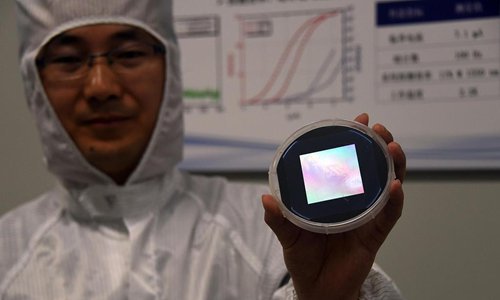
A researcher shows a device produced with the lithography equipment on November 29. Photo: VCG
Researchers with the Chinese Academy of Sciences (CAS) in Southwestern China's Sichuan Province announced their latest breakthrough after setting a new world-record in lithography resolution nanotechnology on November 29, Xinhua News Agency reported.
Vice-Director Hu Song said the breakthrough shatters traditional research methods by creating new pathways in nanometer optical lithography technology, and China now owns the complete intellectual property rights.
Researchers developed lithography equipment that can produce 10-nanometer chips with double exposure technology.
The tests achieved a world record-setting resolution at 22 nanometers developed by researchers with the Institute of Optics and Electronics at CAS.
Scientists at the Technical Institute of Physics and Chemistry said the project establishes a new research direction in the development of high-resolution and large-scale nanometer lithography equipment, surpassing intellectual property barriers set by foreign countries.
Lithography equipment is essential for chip manufacturing, a sector China is now beginning to emerge.
Higher lithography resolution allows increased chip integration levels; while it is hard to increase resolution through traditional lithography technology due to the optical diffraction effect.
Reports said the super-resolution optical lithography equipment has already proven effective in projects at universities and institutions like Shanghai Academy of Spaceflight Technology, University of Electronic Science and Technology of China, West China Hospital and Shanghai Institute of Microsystem and Information Technology.
CAS shatters super-res record with latest lithography equipment
Source:Globaltimes.cn Published: 2018/11/30 2:34:10
A researcher shows a device produced with the lithography equipment on November 29. Photo: VCG
Researchers with the Chinese Academy of Sciences (CAS) in Southwestern China's Sichuan Province announced their latest breakthrough after setting a new world-record in lithography resolution nanotechnology on November 29, Xinhua News Agency reported.
Vice-Director Hu Song said the breakthrough shatters traditional research methods by creating new pathways in nanometer optical lithography technology, and China now owns the complete intellectual property rights.
Researchers developed lithography equipment that can produce 10-nanometer chips with double exposure technology.
The tests achieved a world record-setting resolution at 22 nanometers developed by researchers with the Institute of Optics and Electronics at CAS.
Scientists at the Technical Institute of Physics and Chemistry said the project establishes a new research direction in the development of high-resolution and large-scale nanometer lithography equipment, surpassing intellectual property barriers set by foreign countries.
Lithography equipment is essential for chip manufacturing, a sector China is now beginning to emerge.
Higher lithography resolution allows increased chip integration levels; while it is hard to increase resolution through traditional lithography technology due to the optical diffraction effect.
Reports said the super-resolution optical lithography equipment has already proven effective in projects at universities and institutions like Shanghai Academy of Spaceflight Technology, University of Electronic Science and Technology of China, West China Hospital and Shanghai Institute of Microsystem and Information Technology.
antiterror13
Brigadier
Here the global times news on the same subject via JSCh
CAS shatters super-res record with latest lithography equipment
Source:Globaltimes.cn Published: 2018/11/30 2:34:10
A researcher shows a device produced with the lithography equipment on November 29. Photo: VCG
Researchers with the Chinese Academy of Sciences (CAS) in Southwestern China's Sichuan Province announced their latest breakthrough after setting a new world-record in lithography resolution nanotechnology on November 29, Xinhua News Agency reported.
Vice-Director Hu Song said the breakthrough shatters traditional research methods by creating new pathways in nanometer optical lithography technology, and China now owns the complete intellectual property rights.
Researchers developed lithography equipment that can produce 10-nanometer chips with double exposure technology.
The tests achieved a world record-setting resolution at 22 nanometers developed by researchers with the Institute of Optics and Electronics at CAS.
Scientists at the Technical Institute of Physics and Chemistry said the project establishes a new research direction in the development of high-resolution and large-scale nanometer lithography equipment, surpassing intellectual property barriers set by foreign countries.
Lithography equipment is essential for chip manufacturing, a sector China is now beginning to emerge.
Higher lithography resolution allows increased chip integration levels; while it is hard to increase resolution through traditional lithography technology due to the optical diffraction effect.
Reports said the super-resolution optical lithography equipment has already proven effective in projects at universities and institutions like Shanghai Academy of Spaceflight Technology, University of Electronic Science and Technology of China, West China Hospital and Shanghai Institute of Microsystem and Information Technology.
Great achievement, it seems this baby would match the previous best lithography produced by ASML (just before EUV lithography)
EUV will not be economic for at least a couple of years. Nearly every process over the last decade has involved ArF (193 nm) light sources. Later water immersion and multiple patterning were used to increase feature detail at the expense of system complexity and, with patterning, of wafer output. The industry was supposed to develop CaF2 (157 nm) light sources as a replacement for ArF at the start of this century. But those never entered production, because of difficulties with the technology, they decided to "leap ahead" to EUV and the industry has been stuck on EUV (13.5 nm) light source R&D for like two decades with little progress made in that time period. I think the Japanese manufacturers of lithography tools were among the last to give up on CaF2 light source research. Had that been persisted with we probably could have been making chips with more wafer output right now.
Because they cannot use lower wavelength light sources the industry has had to play with diffraction masks and multiple patterning. But if you use double-patterning, for example, you halve the amount of wafers output per day. This means your factory's production is cut in half. Today it is common to use quadruple-patterning and more. Further reducing wafer output.
Because they cannot use lower wavelength light sources the industry has had to play with diffraction masks and multiple patterning. But if you use double-patterning, for example, you halve the amount of wafers output per day. This means your factory's production is cut in half. Today it is common to use quadruple-patterning and more. Further reducing wafer output.
Last edited:
EUV will not be economic for at least a couple of years. Nearly every process over the last decade has involved ArF (193 nm) light sources. Later water immersion and multiple patterning were used to increase feature detail at the expense of system complexity and, with patterning, of wafer output. The industry was supposed to develop CaF2 (157 nm) light sources as a replacement for ArF at the start of this century. But those never entered production, because of difficulties with the technology, they decided to "leap ahead" to EUV and the industry has been stuck on EUV (13.5 nm) light source R&D for like two decades with little progress made in that time period. I think the Japanese manufacturers of lithography tools were among the last to give up on CaF2 light source research. Had that been persisted with we probably could have been making chips with more wafer output right now.
Because they cannot use lower wavelength light sources the industry has had to play with diffraction masks and multiple patterning. But if you use double-patterning, for example, you halve the amount of wafers output per day. This means your factory's production is cut in half. Today it is common to use quadruple-patterning and more. Further reducing wafer output.
Given that 7nm appears to be the limit for silicon based transistors, am I correct in thinking that a triple pattern of 22nm would produce 7nm chips?