Any state funded research by such institutions such as the CAS or even by major private Chinese entities to attain such capabilities?EUV only uses reflective mirrors not lens due to lens made of fused silica which absorbs EUV light.
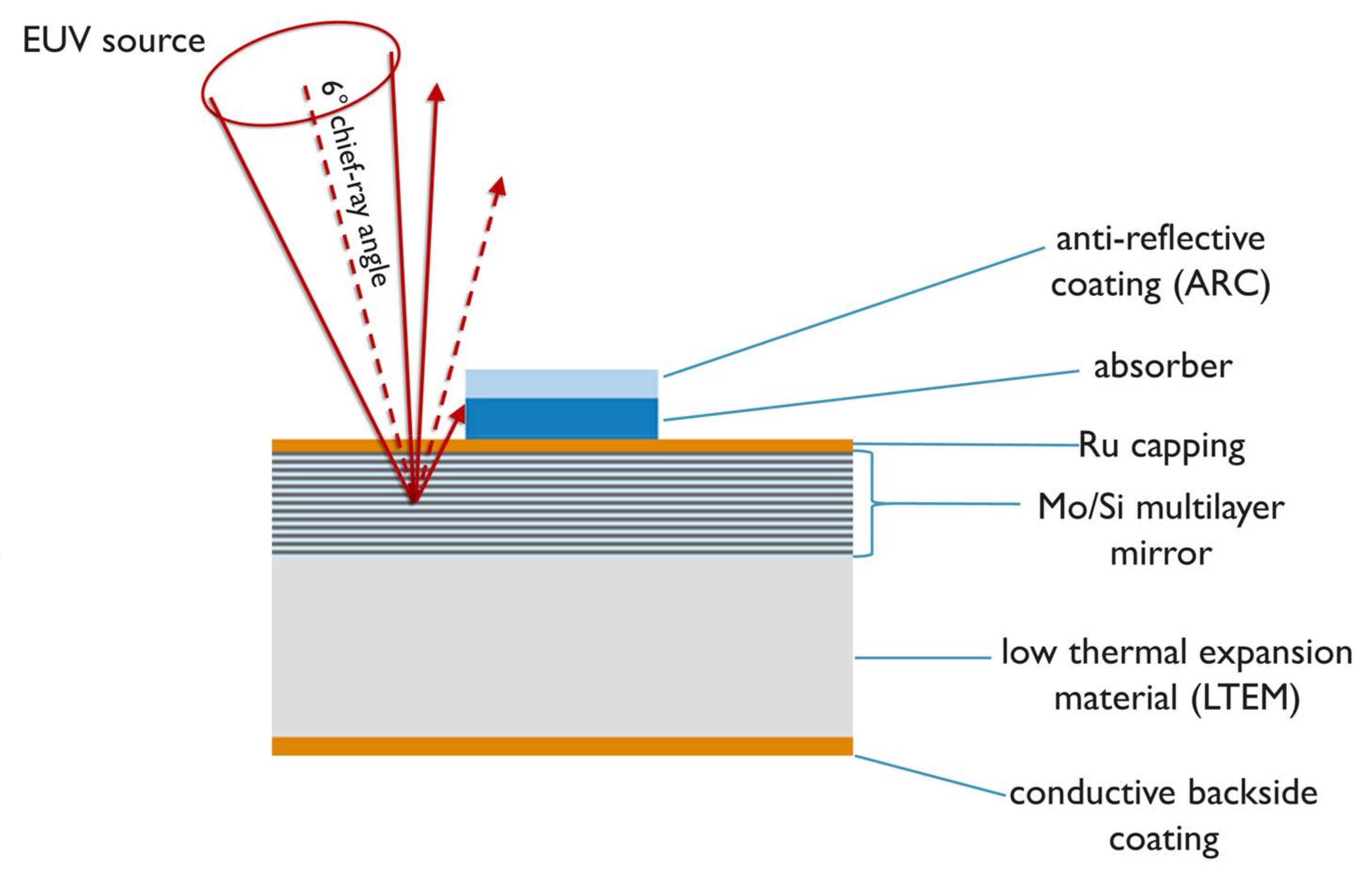
The mirror is about 40 layers of alternate Mo/Si and each layer is 6.8nm thick.
The surface of the mirror has to be very smooth , no more than 0.2nm RMS.. meaning the unevenness of the mirror is a few atoms thick.
0.2nm RMS means only allow 2 atoms difference.
Have to use ion beam to "sand" the layer to remove extra atoms.
That's why its super difficult to make mirror for EUV optics. All optics vendors in China i talked to have not even heard such things ,

You are using an out of date browser. It may not display this or other websites correctly.
You should upgrade or use an alternative browser.
You should upgrade or use an alternative browser.
Germany Carl Zeiss, heart of Dutch ASML Lithography Equipment.
- Thread starter tidalwave
- Start date
- Status
- Not open for further replies.
But it is very informative to all who follow what he shares.This thread is very interesting and I've learned a lot from what tidalwave shared, but does anyone really think anything he publicly disclosed that both the US and Chinese government aren't already fully up to speed and aware of ? It is like a Dan level player watching two Professionals at the game of Go, the Dan player can comment and give outside commentary to the Kyu people watching, but his input wouldn't be of much use to the actual opponents in the game.
One can actually, even though it will come at a substantial cost initially. And given the determination of the US to prevent China from getting access to supplies of equipment, parts, and partially processed materials for ALL high tech industries, and indeed its capability of influencing through enormous pressure that includes threats to foreign countries and suppliers which would otherwise not mind doing business with China, China must actually indeed source its entire supply chain domestically. China must gain the capability to produce anything worth producing within China.People underestimate the difficulty of the semiconductor industry. No one can ever be fully independent in this day n age.
There's a never ending chain of tools that need to be acquired.
Let's use the mirror in the EUV machine for example.
A mirror requires machines that can fabricate it to tight tolerances and software that can design it. You also need to coat it with special materials.
The fabrication machine has to be state of the art. The tools that make that machine is also state of the art. Then there's a never ending chain of machines for each part of that machine.
There are few people that can operate optical design software in this world as it requires physics aptitude (quantum mechanics,...)
The coating requires world experts in chemistry and material sciences. The coating then needs another never ending chain of machines to make it.
You literally have to go from figuring out how to acquire the minerals/chemicals for each part of each machine/material to the final assembly of just a mirror.


I already predict way back that US government will resort to semiconductor equipment banning against Huawei.
That's how my EUV lithography project started about 1 yr ago.
Just as Huawei boasting that it doesnt use US components while at same time switch to TSMC, and use taiwanese and japanese components.
US tech requirement switched from 25% to 10% trying to stop huawei. TSMC quickly said its 7nm and below is below 10% . But that didn't stop there. US government now said anyone use US semiconductor equipment will be subjected to control and this time TSMC will have no way to escape.
The current VC group asking me to provide guidance how to achieve EUV lithography doesn't have the vast funding to make it happen. It needs alot of tools that China yet to develope . ANyway, I give them quite detailed presentation on what tools needed to get in order to get EUV project started.
I was trying reach Huawei, i told them hey now, you are blacklisted by US government, you can't just do business as usual, can't just outsource somewhere and have others manufacture for them. Huawei needs to proactively get invovled in mnufacturing and even chinese semiconductor equipment devleopment. Their response still kind of buearucratic.
I think this time, Huawei will get hit against the wall.
I already predict way back that US government will resort to semiconductor equipment banning against Huawei.
That's how my EUV lithography project started about 1 yr ago.
Just as Huawei boasting that it doesnt use US components while at same time switch to TSMC, and use taiwanese and japanese components.
US tech requirement switched from 25% to 10% trying to stop huawei. TSMC quickly said its 7nm and below is below 10% . But that didn't stop there. US government now said anyone use US semiconductor equipment will be subjected to control and this time TSMC will have no way to escape.
The current VC group asking me to provide guidance how to achieve EUV lithography doesn't have the vast funding to make it happen. It needs alot of tools that China yet to develope . ANyway, I give them quite detailed presentation on what tools needed to get in order to get EUV project started.
I was trying reach Huawei, i told them hey now, you are blacklisted by US government, you can't just do business as usual, can't just outsource somewhere and have others manufacture for them. Huawei needs to proactively get invovled in mnufacturing and even chinese semiconductor equipment devleopment. Their response still kind of buearucratic.
I think this time, Huawei will get hit against the wall.
Huawei and a China have no choice but to completely self reliant in all areas of high tech capabilities.
What makes s
What high end IC semiconductors and semiconductor manufacturing equipment so difficult? Is it the lack of proper application when attempting to make the products?
I already predict way back that US government will resort to semiconductor equipment banning against Huawei.
That's how my EUV lithography project started about 1 yr ago.
Just as Huawei boasting that it doesnt use US components while at same time switch to TSMC, and use taiwanese and japanese components.
US tech requirement switched from 25% to 10% trying to stop huawei. TSMC quickly said its 7nm and below is below 10% . But that didn't stop there. US government now said anyone use US semiconductor equipment will be subjected to control and this time TSMC will have no way to escape.
The current VC group asking me to provide guidance how to achieve EUV lithography doesn't have the vast funding to make it happen. It needs alot of tools that China yet to develope . ANyway, I give them quite detailed presentation on what tools needed to get in order to get EUV project started.
I was trying reach Huawei, i told them hey now, you are blacklisted by US government, you can't just do business as usual, can't just outsource somewhere and have others manufacture for them. Huawei needs to proactively get invovled in mnufacturing and even chinese semiconductor equipment devleopment. Their response still kind of buearucratic.
I think this time, Huawei will get hit against the wall.
What high end IC semiconductors and semiconductor manufacturing equipment so difficult? Is it the lack of proper application when attempting to make the products?
They have skipped alot of steps. Alot of fundamental tools they haven't developed yet.What makes s
What high end IC semiconductors and semiconductor manufacturing equipment so difficult? Is it the lack of proper application when attempting to make the products?
Before they even do EUV , they got to do focus ion beam that can make edits to the nanostructure of circuits.
Then a host of specialty interferometer for surface measurement. Profile measurement tools.
In EUV, they need develope high power laser system, mirrors.
I find out alot of those Chinese academy of science people are taking easy out, getting grants from government funding and all they do is copy some western papers and maybe have some of their inputs, mostly in theoretical thing and publish them and calling that's their works. They don't really build real system.
I read a bunch of their works on EUV. All are theoretical stuffs.
They have skipped alot of steps. Alot of fundamental tools they haven't developed yet.
Before they even do EUV , they got to do focus ion beam that can make edits to the nanostructure of circuits.
Then a host of specialty interferometer for surface measurement. Profile measurement tools.
In EUV, they need develope high power laser system, mirrors.
I find out alot of those Chinese academy of science people are taking easy out, getting grants from government funding and all they do is copy some western papers and maybe have some of their inputs, mostly in theoretical thing and publish them and calling that's their works. They don't really build real system.
I read a bunch of their works on EUV. All are theoretical stuffs.
Did you email him directly about it
[email protected]
[email protected]
- Status
- Not open for further replies.