Chinese semiconductor thread II

tokenanalyst

Lieutenant General
Registered Member

Mingtai Microelectronics Advanced Packaging and Testing Project Tops Out with 500 Million Yuan Investment


On July 17, 2026, Sichuan Mingtai Microelectronics announced that the main structure of its Phase II advanced packaging and testing production project has been successfully topped out. This milestone marks a significant breakthrough in the company’s strategy to expand capacity and upgrade technology, injecting new momentum into the integrated circuit (IC) industry cluster in Neijiang, Sichuan.

The project involves a total investment of 500 million yuan (~$70 million USD), covers an area of 25 mu (approx. 1.67 hectares), and has a total construction area of 45,000 square meters. It is a key regional initiative aimed at strengthening high-end IC packaging and testing capabilities. Upon completion, the facility will feature high-standard cleanrooms and introduce advanced equipment, including fully automated packaging lines and high-precision intelligent testing devices. This will significantly enhance production accuracy, efficiency, and competitiveness in the high-end chip market.

Construction began in November 2025. The project is scheduled for full completion and delivery by February 2027. Once operational, the project will add an annual capacity of over 10 billion high-end IC packages, helping to fill the regional gap in advanced packaging capacity. It is expected to generate an annual output value exceeding 1.5 billion yuan and create more than 2,000 local jobs, further strengthening the regional semiconductor supply chain and talent pool.

Mingtai Microelectronics is a national high-tech enterprise engaged in the packaging and testing of integrated circuits and discrete devices . It is currently the largest independent third-party packaging and testing service provider in the Chengdu-Chongqing economic circle. Its main business is the packaging, testing, and sales of integrated circuits and power devices, and it is the largest independent third-party foundry in Southwest China. The company's existing packaging products mainly include DIP series, SOP series, TO series, SOT series, QFN/DFN, LQFP, LGA, PDF
Please, Log in or Register to view URLs content!
 

tokenanalyst

Lieutenant General
Registered Member

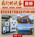
Shenggong Co., Ltd. invested 1.13 billion yuan to build silicon component and other projects.​


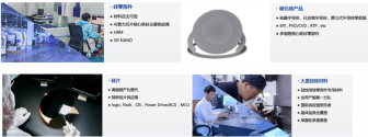
Jinzhou Shenggong Semiconductor Co., Ltd. (stock code: 688233, stock abbreviation: Shenggong) issued an announcement stating that it plans to invest a total of approximately RMB 1,129,921,400 (subject to actual investment) to construct a new silicon component R&D and supporting silicon material capacity expansion project, a key integrated circuit manufacturing material R&D and industrialization project, and a new packaging and micro-nano optoelectronic silicon material R&D and industrialization project. Specifically, the planned investment for the "New Silicon Component R&D and Supporting Silicon Material Capacity Expansion Project" is RMB 586,498,000; the planned investment for the "Key Integrated Circuit Manufacturing Material R&D and Industrialization Project" is RMB 325,626,300; and the planned investment for the "Packaging and Micro-nano Optoelectronic Silicon Material R&D and Industrialization Project" is RMB 217,797,100. The above project amounts are estimated values under the current plan. Shenggong will invest in stages as needed based on project progress, market environment, and financial situation. The specific investment scale and implementation pace will be dynamically adjusted according to actual circumstances, and the final amount will be based on the actual amount incurred.

The semiconductor industry is rapidly evolving, with demand for silicon-based materials in packaging and micro-nano optoelectronics continuously expanding, creating vast potential for domestic substitution of high-end silicon components. Shenggong Technology's core business currently focuses on large-diameter silicon materials and silicon components, with products primarily used by silicon component equipment manufacturers, downstream semiconductor etching equipment manufacturers, and terminal memory chip manufacturers.

1784318164405.png


Shenggong Technology's existing production capacity and product range are insufficient to fully cover the diversified and high-end procurement needs of downstream customers, resulting in shortcomings in capacity supply and new product development capabilities. The simultaneous deployment of these three projects will complement and improve Shenggong Technology's comprehensive integrated circuit material product matrix, allowing it to seize opportunities in the domestic substitution industry, enhance its self-sufficiency in high-end semiconductor materials, consolidate its market share, and support the company's long-term strategic development. Shenggong Technology has been deeply involved in silicon components for many years, possessing a mature R&D team, stable downstream customer resources, and mature production processes, with accumulated technical expertise in new material R&D and large-scale mass production. The project sites are primarily located in Jinzhou, a region with a well-developed semiconductor industry and strong policy support; funding comes from its own capital and self-raised funds, with readily available financing channels. Each project is being constructed in phases and stages, with short-term and long-term production capacity being released in an orderly manner. The R&D and production line construction plans have been fully demonstrated, and the technology, site, funding, and market conditions are all in place for implementation, making the projects highly feasible.

Please, Log in or Register to view URLs content!
 

tokenanalyst

Lieutenant General
Registered Member

High-precision primary mirror testing for large-aperture dynamic interferometers based on projection distortion correction​

Abstract:​

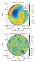
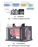
A large-aperture Twyman–Green dynamic interferometer employs a high-precision primary mirroras its core component. Projection distortion between measured wavefront and actual surface figure of the mirror must be corrected to ensure the accuracy and efficiency of primary mirror’s compensation fabrication. To address issues of cumbersome and complex distortion correction methods that often neglect influence of internal optical path of interferometer, a correction method combining affine transformation and radial distortion modeling was proposed. Using a small number of targets and a coordinate measuring machine (CMM), an affine model was established. Through secondary programming development based on interface of optical design software, large-scale ray tracing and radial distortion fitting were performed to reconstruct interferometric wavefront distribution quickly and accurately. A decoupling method between alignment errors and surface figure errors after distortion correction was also analyzed. The proposed method was applied to correct projection distortion in compensation test results of an aspheric primary mirror with an effective aperture of Φ450 mm. Based on corrected results, magnetorheological finishing compensation of primary mirror was guided. The interferometric cavity wavefront root mean square (RMS) converged from 0.109 3λ to 0.010 4λ, which decreased by 90.48%, outperformed the convergence ratio achieved without distortion correction. Experimental results validate the effectiveness of the proposed method.

1784319649259.png1784319678447.png

Please, Log in or Register to view URLs content!
 

tokenanalyst

Lieutenant General
Registered Member

China Reform Fund leads investment in Aixin Semiconductor, boosting new breakthroughs in the field of domestic semiconductor quality inspection equipment.​


Guofengtou Beijing Intelligent Manufacturing Fund and Guofengtou New Wisdom Fund, subsidiaries of the Guoxin (China Reform) Fund, have jointly led the Series B+ financing round for Shenzhen Aixin Semiconductor Technology Co., Ltd. This strategic investment underscores the fund's commitment to supporting domestic semiconductor advancements, with a specific focus on high-end metrology equipment essential for the integrated circuit industry chain. The funding aims to accelerate technological iteration and industrial application, reinforcing the company’s position in tackling critical "bottleneck" challenges within advanced process equipment.

Founded in 2020, Aixin Semiconductor has established itself as a national-level specialized and innovative "Little Giant" enterprise by developing core technology systems in optics and X-ray for wafer measurement and inspection. The company’s independent R&D efforts have produced equipment adaptable to various mainstream chip manufacturing processes, including logic and memory chips. Recognized as a potential unicorn and home to provincial engineering research centers, Aixin Semiconductor focuses on overcoming technical barriers through continuous innovation, providing downstream customers with high-quality, cost-effective, and localized solutions that benchmark against leading international products.

1784322202923.png

Investment in Aixin Semiconductor serves as a key initiative for the China Reform Fund to implement national integrated circuit development strategies and leverage state-owned capital for industrial upgrading. Fund representatives highlighted the company’s ability to fill industrialization gaps in domestic high-end metrology equipment through its stable product performance and strong technical capabilities, which have earned recognition from leading downstream customers. By utilizing its ecosystem resources, the fund intends to empower Aixin Semiconductor to achieve high-quality development, further promoting the localization of critical semiconductor technologies and ensuring the safe, stable growth of the industry chain.

Please, Log in or Register to view URLs content!
 

tokenanalyst

Lieutenant General
Registered Member

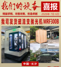
China Reform Fund leads investment in Shanxi Zhongdian Technology Co., Ltd., to support the localization of high-temperature purification equipment manufacturing and purification technology​


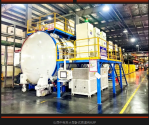
China Reform Fund’s Central Enterprise Strategic Emerging Industries Fund has led the B-round investment in Shanxi CETC Electronic Equipment Co., Ltd., a manufacturer specializing in high-temperature purification and coating systems for semiconductor materials. Founded in 2010, the company develops critical equipment and processing technologies for essential substrates including high-purity graphite, electronic-grade oxygen-free copper, silicon carbide coatings, and semiconductor quartz products. Through sustained research and industrial validation, Shanxi CETC has successfully advanced domestic production capabilities in these strategic sectors, holding 198 patent applications with 100 officially granted, comprising invention and utility model patents that support its commercial-scale manufacturing programs.

1784323433767.png


Company leadership stated that the investment validates progress in overcoming critical technology bottlenecks within domestic equipment manufacturing. Building on state-owned backing and national research platforms, Shanxi CETC intends to accelerate the transition from laboratory development to stable mass production. The company will continue refining silicon carbide coating systems and ultra-high-temperature purification tools while delivering integrated solutions that combine hardware, process engineering, and technical support to advance China’s third-generation semiconductor and advanced materials industries.

According to the fund’s investment leadership, high-end purification and coating equipment is fundamental to maintaining semiconductor material quality and supply chain resilience. Shanxi CETC has established itself as a domestic leader by breaking foreign monopolies through targeted research, proven project execution, and comprehensive industrial verification. This funding aligns with national industrial strategy by strengthening local capabilities in core semiconductor manufacturing tools and accelerating the adoption of domestically produced alternatives across the technology supply chain.
Please, Log in or Register to view URLs content!
 

tokenanalyst

Lieutenant General
Registered Member

IdoNano Focusing on the research and development of domestically produced high-end X-ray diffractometers , showcased innovative achievements.​


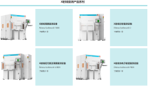
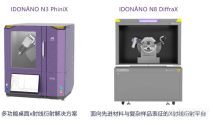
During the exchange, the IdoNano team introduced the company's technological research and development work on domestically produced high-performance X-ray diffractometers to Dean Sun Zhenrong and his delegation, and highlighted the N3 series benchtop X-ray diffractometers and the N8 DiffraX X-ray diffraction platform for characterizing advanced materials and complex samples.
1784323863143.png


CEO of the company, introduced that since its establishment, IdoNano has been focusing on the localization of high-end X-ray diffraction instruments and carrying out technological research and development around the material structure analysis needs of key industrial fields such as advanced materials, semiconductors, and new energy.

In response to the application needs of key material structure analysis, thin film and complex structure system characterization in advanced semiconductor manufacturing processes, the company focuses on promoting the development of the N8 DiffraX platform for the semiconductor metrology field . It conducts technical research and development in key areas such as high-resolution X-ray optical systems, precision motion control, high-performance detection technology and intelligent data analysis, and explores the development path of domestic high-end semiconductor material analysis and metrology equipment.​


Please, Log in or Register to view URLs content!
 
Top