How much is YMTC’s capacity based on domestic tooling?not sure about NAURA, but AMEC has reported it's getting pretty close on 90:1 etcher. YMTC has been working on tuning its all domestic production line for a while now and supposedly will start production soon. So, nothing too surprising here.
UBS is late to the game
You are using an out of date browser. It may not display this or other websites correctly.
You should upgrade or use an alternative browser.
You should upgrade or use an alternative browser.
Chinese semiconductor thread II
- Thread starter vincent
- Start date
They have a previous 3D-NAND etcher
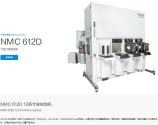
Looking a my previous post, Naura launched a series of new tools, "secretly". One of those says is a Deep Silicon Etcher for 3D-NAND Above Generation 5, I don't know how the generation translate to the number of layers. I think is over the hundreds.

Looking a my previous post, Naura launched a series of new tools, "secretly". One of those says is a Deep Silicon Etcher for 3D-NAND Above Generation 5, I don't know how the generation translate to the number of layers. I think is over the hundreds.
I have notice that Naura has quietly been adding semiconductor tools to their catalog.
The Landscape: A plasma etching-doping system that implant Ions into junctions and trenches of ICs, different from Ion implanters that accelerate particles using magnets this looks likes use energy of the plasma field to implant the atoms. The equivalent would be AMAT VIISta
View attachment 163562
The ACCURA Family: already discuss here, for deep hole-trench, dielectric etching and 3D-NAND
View attachment 163563
The Surefill W Family: For Tungsten thin film Chemical Deposition for the interconnects in ICs, my guess is to compete with AMAT Endura, especially with AMEC Preforma Uniflex.
View attachment 163564
They Also entered the Ion Implantation business, the Sirius family and the Rapid Thermal Processing business with the Sitara family probably to complement their Ion Implanters, RPT tools are used after Ion Implantation basically recrystallize the atoms after doping.
View attachment 163566
Tuojing Technology plans to jointly invest in Chipone Precision with related parties.
Tuojing Technology plans to jointly invest with its related party, Fengquan Venture Capital (in which senior executives including Chairman Lu Guangquan and Director Liu Jing are limited partners), in Ningbo Xinfeng Precision Technology Co., Ltd. (Xinfeng Precision). This constitutes a related-party transaction.Tuojing Technology will acquire up to RMB 270 million for 16.42% of Xinfeng Precision’s registered capital (equivalent to RMB 9.9838 million in registered capital). Fengquan Venture Capital will invest RMB 30 million for 1.82% of the company's capital (RMB 1.1093 million in registered capital).
Xinfeng Precision’s specializes in thinning, dicing, and cutting equipment and consumables for 3D IC and advanced packaging processes. Has independent R&D and manufacturing capabilities for core software and components. Both companies operate in semiconductor equipment Tuojing focuses on advanced bonding and metrology equipment for 3D integration, while Xinfeng provides key processing tools.
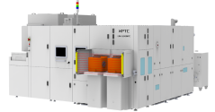
The investment strengthens Tuojing Technology's industrial ecosystem and synergies with Xinfeng Precision, especially in the 3D integration process where thinning, dicing, and bonding are closely interdependent.
Horizon Robotics unveils 4th gen BPU architecture for Journey 7 series of chips. Expecting this to allow 10x higher compute & 5x better power efficiency.
凌光红外/Luxet Infrared has developed OBIRCH machine called LaserSight-100 (+ full LaserSight series). Its suitable for detecting defection caused by metal interconnects, metal/semi short circuits. It's a power semi failure analysis tech using scanned laser beam. Multiple units have already bee delivered & matches imported equipment. Hamamatsu Photonics seems like the biggest player here.
Shengmei Shanghai: Several equipment models adapted to HBM process have been launched.
On December 8, ACM Shanghai announced the launch of several equipment models specifically adapted for the High Bandwidth Memory (HBM) process. Key products include:
- Ultra ECP 3D: A core electroplating device for TSV copper filling, capable of processing 3D NAND with over 500 layers at a yield of 99.8%, supporting sub-5nm processes and with an annual capacity of 30 units. It has already entered Samsung’s supply chain and is designed for high-aspect-ratio TSV structures.
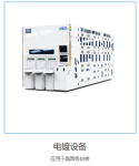
- Wet Cleaning & Copper Plating Equipment: Multiple independently developed cleaning systems, including:
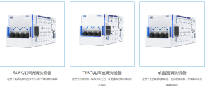
- SAPS megasonic technology for deep TSV cleaning, reducing leakage current by 2–3 orders of magnitude; used in SK Hynix and Micron production lines.
- World’s first TEBO megasonic system, verified by leading chipmakers and already sold to four customers.
- Ultra C Tahoe, offering fine cleaning with up to 75% sulfuric acid savings.
- Supercritical CO₂ cleaning/drying, enabling non-destructive, non-adhesive processing for ultra-fine HBM structures.
- Packaging & Testing Equipment: Full range of wet, coating, developing, and copper plating tools compatible with both HBM and 2.5D packaging. The company’s FOPLP electroplating equipment supports large substrates (610×457mm), meeting high-density AI chip needs and is at international leading levels.
- Invest 250 million yuan in advanced wet processing for HBM wafer bonding.
- Allocate 820 million yuan to PECVD equipment and develop ALD technology targeting single-atom-level dielectric precision by 2026.
- Launch cleaning equipment for HBM4 by 2026.
- Establish a dedicated HBM R&D lab in South Korea.
The Institute of Microelectronics has made significant progress in heterogeneous integration of GaN HEMT based on 4H-SiC/Diamond composite substrates.
The Institute of Microelectronics, led by Professor Liu Xinyu, has developed a breakthrough in GaN HEMT technology using a 4H-SiC/diamond composite substrate to solve severe heat dissipation issues in high-power devices. Traditional substrates like Si or SiC struggle with thermal management under rising device power and voltage, limiting performance and reliability.
The team introduced a surface-activated bonding (SAB)-based secondary transfer technique to bond a 784 nm thick 4H-SiC film onto a diamond substrate enabling high-temperature GaN epitaxy while reducing lattice and thermal mismatch. The process achieved up to 98% bonding efficiency, with the transferred SiC film maintaining excellent crystal quality (FWHM comparable to bulk SiC).
After annealing at 900°C, the interface thermal resistance dropped to 13.6 m²·K/GW the best reported value for 4H-SiC/diamond interfaces due to elimination of an amorphous layer and local recrystallization.
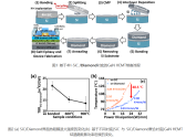
Experimental results show that GaN HEMTs on this composite substrate exhibit:
- 61.4% lower thermal resistance
- 40.5°C reduced junction temperature (at 23.4 W/mm²)
This demonstrates significantly improved heat dissipation, reliability, and power performance while preserving process compatibility. The solution holds strong potential for next-generation high-frequency, high-power applications such as 5G/6G communications, satellite systems, and radar.
yeah, I posted this story a few days ago, but it's pretty good stuff. Shows that SiC/Diamond substrate allows significantly higher power before overheating. So this is really great stuff for CETC in those GaN radar applications.The Institute of Microelectronics has made significant progress in heterogeneous integration of GaN HEMT based on 4H-SiC/Diamond composite substrates.
The Institute of Microelectronics, led by Professor Liu Xinyu, has developed a breakthrough in GaN HEMT technology using a 4H-SiC/diamond composite substrate to solve severe heat dissipation issues in high-power devices. Traditional substrates like Si or SiC struggle with thermal management under rising device power and voltage, limiting performance and reliability.
The team introduced a surface-activated bonding (SAB)-based secondary transfer technique to bond a 784 nm thick 4H-SiC film onto a diamond substrate enabling high-temperature GaN epitaxy while reducing lattice and thermal mismatch. The process achieved up to 98% bonding efficiency, with the transferred SiC film maintaining excellent crystal quality (FWHM comparable to bulk SiC).
After annealing at 900°C, the interface thermal resistance dropped to 13.6 m²·K/GW the best reported value for 4H-SiC/diamond interfaces due to elimination of an amorphous layer and local recrystallization.
View attachment 165951
Experimental results show that GaN HEMTs on this composite substrate exhibit:
Yes is pretty interesting. Higher power with minimal thermal solutions will allow radars to have longer range and better resolution while be more compact. The benefits for autonomous driving could be interesting allowing better time reactions.yeah, I posted this story a few days ago, but it's pretty good stuff. Shows that SiC/Diamond substrate allows significantly higher power before overheating. So this is really great stuff for CETC in those GaN radar applications.
For the military could allow longer range missiles due less thermal hardware and higher power.

