South Korea being controlled by powerful companies like Samsung is so depressing for the entire country, glad it's the other way round for China. Even the most powerful companies in China are under the government's watchful observation.I think it's just samsung using their control over the government to scare employees against jumping ship. All south koreans can only be slaves to samsung
You are using an out of date browser. It may not display this or other websites correctly.
You should upgrade or use an alternative browser.
You should upgrade or use an alternative browser.
Chinese semiconductor thread II
- Thread starter vincent
- Start date
US is busy coping about its failure.
SAN FRANCISCO, Oct 7 (Reuters) - Gaps in efforts by the U.S. and allies to restrict China's ability to manufacture advanced computing chips have allowed China to buy nearly $40 billion of sophisticated chipmaking gear, according to a bipartisan investigation by U.S. lawmakers.
But inconsistencies in rules issued by the United States, Japan and the Netherlands have led to non-U.S. toolmakers selling to some Chinese firms that U.S. companies could not, according to a report by the U.S. House of Representatives Select Committee on China seen by Reuters.
Chinese firms last year bought $38 billion in equipment from five top semiconductor manufacturing equipment suppliers, without breaking the law, a 66% increase from 2022, when many of the tool export restrictions were introduced. It also accounted for nearly 39% of the aggregate sales of Applied Materials , Lam Research , KLA , ASML and Tokyo Electron , the report found.
I think there is a probability that the overpaid stooges in Washington D.C are going to make the entire US semiconductor industry to collapse, i think even probably in the near future. The US doesn't have a effective industrial policy, the entire tech ecosystem is relying in a tech bubble and on top there are so many export restrictions to US companies to sell to a big market like China that any pop of the bubble is going to hit these companies really hard and the US market will probably no be able to compensate for the lost of a big market like China.
The vast majority of Nvidia revenue depend on just a few companies. If the AI chat bubble pops, there goes Nvidia and then TSMC and then KLA, AMAT, LAM and ASML, all the way down to coffee machines. And that is not counting that Intel is down pretty bad and their recovery is uncertain. Usually these companies could rely on a Market like China who has a more diverse tech ecosystem, they don't only want chips for datacenters but also for humanoid robotics, self-driving vehicles, 5G and the extensive list goes on. Also Chinese generative AI labs focus on open source and efficient solutions allows medium and small businesses to implement custom solutions that will probably boost sales of GPUs and AI hardware. That is why Jensen is concerned about losing the Chinese market because the cloud closed approach of US labs make them rely on a shrinking pool of costumers for their GPUs.
The vast majority of Nvidia revenue depend on just a few companies. If the AI chat bubble pops, there goes Nvidia and then TSMC and then KLA, AMAT, LAM and ASML, all the way down to coffee machines. And that is not counting that Intel is down pretty bad and their recovery is uncertain. Usually these companies could rely on a Market like China who has a more diverse tech ecosystem, they don't only want chips for datacenters but also for humanoid robotics, self-driving vehicles, 5G and the extensive list goes on. Also Chinese generative AI labs focus on open source and efficient solutions allows medium and small businesses to implement custom solutions that will probably boost sales of GPUs and AI hardware. That is why Jensen is concerned about losing the Chinese market because the cloud closed approach of US labs make them rely on a shrinking pool of costumers for their GPUs.
Local suppliers of silicon wafers are rapidly gaining market share.
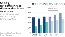
"When verification was completed in the past year or two, the majority of local chipmakers largely switched to producing chips on domestically made silicon wafers. The shift is quite significant," said one executive with direct knowledge of the situation. "Regardless if you are a Chinese supplier of driver chips or not, if you want China's business, it is strongly 'encouraged' to use Chinese-made wafers," an executive with a display and semiconductor equipment manufacturer told Nikkei Asia. "This is also the way China's self-sufficiency policy can sustain itself."
David Dai, a veteran semiconductor analyst at Bernstein Research, said China's pace of achieving self-sufficiency in silicon wafers is picking up faster than many outsiders had expected, especially for more mature, or older generation, chips. "Global market leaders' share in China is bound to decline. The country's self-sufficiency in 12-inch wafers has already reached more than 50% when looking only at supplies to local Chinese chipmakers and excluding foreign chipmakers, such as Samsung, TSMC or SK Hynix, that operate plants in China," Dai said. "For 8-inch wafers, self-sufficiency rates are already 80%. In memory chipmaking cases, the percentage is even higher."

From Huawei Whisper
Kirin9030 is very good and do not need a fan, I assume that's in reference to much lower heating issues. Expect to be launched in Nov.9030很好 无需风扇 新系统新技术新惊喜
下月见
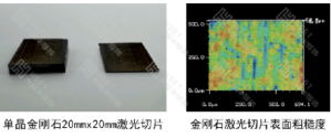
Han's Semiconductor achieves major breakthrough in diamond QCBD laser slicing technology
Han's Semiconductor, a subsidiary of Han's Laser, has achieved a major breakthrough in diamond laser slicing technology, addressing one of the most persistent challenges in advanced semiconductor manufacturing: how to efficiently and precisely process ultra-hard diamond materials. As diamond’s exceptional thermal conductivity, wide bandgap, and high carrier mobility make it ideal for next-generation electronics and quantum devices, demand for its use continues to grow. However, diamond’s extreme hardness makes traditional mechanical cutting methods inefficient, resulting in high material loss, low yield, and costly defects barriers that have hindered large-scale industrial adoption.
The breakthrough lies in Han's proprietary Quantum-Crystal Boundary Diamond (QCBD) laser slicing technology, which uses ultrafast lasers to non-contactingly modify diamond’s internal structure. By precisely focusing laser energy at a subsurface depth, the process induces controlled physicochemical changes that create a weak layer, allowing external stress to guide crack propagation along a predefined plane. This enables clean, high-precision separation without mechanical damage critical for maintaining crystal integrity and surface quality. Unlike silicon carbide, diamond’s cleavage plane ({111}) is at a significant angle to the slicing direction ({100}), making process control more complex; Han's technology overcomes this through precise laser energy modulation and beam shaping.
Han’s QCBD technology has demonstrated impressive performance metrics: peeling surface roughness (Ra) of less than 3μm, with a laser-damaged layer reduced to just 20μm. This precision significantly enhances material yield and reduces waste while improving processing efficiency. These results represent a substantial leap from conventional methods and mark China’s first major advancement in commercial diamond laser slicing technology, filling a critical gap in domestic high-end semiconductor manufacturing capabilities.
The implications of this breakthrough are far-reaching. By slashing production costs and enabling scalable, high-quality diamond wafer fabrication, the QCBD technology opens doors for broader use in high-performance electronics, quantum computing, and advanced optical systems. With further development, it could transform the diamond materials industry, accelerating its integration into cutting-edge technologies and ushering in a new era of efficient, precise semiconductor material processing.
Huawei HiSilicon's high-performance VCSEL helps create high-quality Xingyun optical interconnect solutions
Leveraging years of experience in multi-mode VCSELs, HiSilicon has developed the StarMatrix optical interconnect solution from the perspectives of product definition, architecture design, and system reliability. This solution incorporates key optical chip specifications into the top-level design of optical modules. Through high-quality epitaxial growth and process control technologies, HiSilicon comprehensively ensures the performance and long-term stability of optical chips, providing high-quality StarMatrix optical interconnect products for AI intelligent computing networks.
The 50Gbps VCSEL is compatible with the Nebula 400G optical interconnect solution, extending the multimode optical interconnect distance to 200m. Leveraging its proprietary, mature 6-inch GaAs IDM platform, ultra-high-precision epitaxial growth control, and full-process AI process defect monitoring and interception capabilities, it combines high-performance margin with ultra-high reliability, extending the optical interconnect distance to 200m and ensuring the Nebula 400G optical interconnect solution boasts the best overall performance in the industry.
100Gbps VCSELs power the Nebula 800G optical interconnect solution, enabling multimode optical interconnects up to 150m. Through comprehensive optimization at the chip material and module system levels, the Nebula 800G optical interconnect solution achieves stable transmission over 100m, delivering excellent fiber transmission performance. Furthermore, based on the underlying VCSEL mechanism, further optimizations in bandwidth and spectrum width, coupled with industry-leading improvements in effective mode bandwidth, support optical interconnect distances up to 150m, adapting to the needs of larger-scale cluster interconnection scenarios.
200Gbps VCSELs support 50m transmission, underpinning the continued evolution of Nebula Optical Interconnect. By leveraging material limitations, innovating chip architectures, and balancing multiple key parameters, they enable stable 200G VCSEL transmission over traditional OM4 fiber. Combined with the introduction of higher effective mode bandwidth fiber, transmission distances reach 50m. HiSilicon's 18-channel, high-density multimode VCSEL array provides a cost-effective solution for the continued evolution of future high-capacity AI scale-up networks.
SMEE got a patent for their high speed reticle scanning device
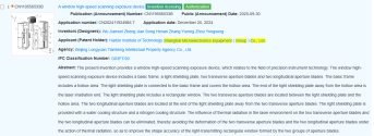
Plus filled an EUV patent.
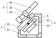
Tianyancha shows that the patent of "A beam adjustment device and photolithography machine" of Shanghai Micro Electronics Equipment (Group) Co., Ltd. has been announced. The application publication date is March 21, 2025, and the application publication number is CN119668039A.
The present invention relates to the field of semiconductor manufacturing technology, and in particular to a beam adjustment device and a photolithography machine. The beam adjustment device includes a support seat, a reflective mirror group, and a driving mechanism. The reflective mirror group includes a mirror group mounting seat and a mirror group fixed to the mirror group mounting seat. The center position of the mirror group mounting seat is movably connected to the support seat. The driving ends of the two driving mechanisms are perpendicular to the line connecting the center positions of the mirror group mounting seats. The driving end of one driving mechanism can drive the mirror group mounting seat to rotate around a first axis, and the driving end of the other driving mechanism can drive the mirror group mounting seat to rotate around a second axis. The first axis is perpendicular to the second axis, thereby realizing the separate control of the rotation in the direction of the first axis and the rotation in the direction of the second axis, avoiding crosstalk between the rotations in the two directions, and improving the control accuracy. By applying the above-mentioned beam adjustment device, the photolithography machine has good processing quality and high product yield.

From Huawei Whisper
Kirin9030 is very good and do not need a fan, I assume that's in reference to much lower heating issues. Expect to be launched in Nov.
Isn't Kirin 9030 a phone CPU like the Kirin 9020 and 9010? Vast majority of phones don't have fans, with the only exceptions being some hardcore gaming phones.
Kirin 9010 and 9020 have also been used on smart TV, pad and kirin series likely will be used on laptop also.Isn't Kirin 9030 a phone CPU like the Kirin 9020 and 9010? Vast majority of phones don't have fans, with the only exceptions being some hardcore gaming phones.
