Chinese semiconductor thread II

tokenanalyst

Brigadier
Registered Member

Huahai Qingke's 12-inch thinning and film laminating machine Versatile-GM300 is shipped in batches to leading domestic semiconductor companies​


  Recently, the 12-inch thinning and film bonding machine Versatile-GM300 independently developed by Huahai Qingke Co., Ltd. (referred to as "Huahai Qingke") has achieved batch shipments and has been continuously shipped to many leading domestic semiconductor companies. This marks that the equipment has officially entered the stage of large-scale application, injecting new momentum into the domestic high-end semiconductor packaging field.

1751318681683.png

Versatile-GM300 integrates the functions of grinding and thinning, polishing to relieve stress, stripping protective film and pasting dicing film, realizing full-process automation, significantly reducing the risk of processing damage, and improving efficiency and yield. The equipment can perform ultra-thin processing on Single Wafer, and is perfectly compatible with the two mainstream advanced packaging process routes of Wafer to Wafer (W2W) and Die to Wafer (D2W), providing a reliable and flexible solution for the last backside thinning process before product packaging.

At present, Versatile-GM300, together with Huahai Qingke's independently developed edge trimming machine Versatile-DT300 , thinning and polishing all-in-one machine Versatile-GP300 , and CMP series equipment Universal-300 Dual/X/T, form a complete set of 3D IC solutions , which can better meet the urgent needs of cutting-edge technology fields such as AI chips, HBM (high bandwidth memory) stacked packaging, and Chiplet (core particle) heterogeneous integration.

1751318658432.png

 The successful mass production and sales of Versatile-GM300 is an important achievement of Huahai Qingke's continuous deepening of the "equipment + service" platform development strategy, which effectively fills the key link of the domestic integrated circuit industry chain. In the future, Huahai Qingke will continue to uphold the corporate spirit of "self-reliance to achieve excellence and innovation to shape the future", and is committed to providing customers with more efficient and advanced semiconductor complete solutions, actively developing new quality productivity through technological innovation, and promoting the high-quality development of China's semiconductor industry.​

Please, Log in or Register to view URLs content!
 

tokenanalyst

Brigadier
Registered Member

Coherent Compton scattering using a stretched off-axis paraboloid​

Abstract​

Extreme ultraviolet (EUV) lithography is crucial for advancing semiconductor manufacturing; however, current EUV light sources, such as laser-produced plasma (LPP), have significant limitations, including low energy-conversion efficiency and debris contamination. Various schemes, including optical free-electron laser undulators, have been studied to generate coherent EUV light. However, optical undulators suffer from limited focal lengths, which pose a significant challenge to achieving a higher gain. In this study, a novel approach is proposed that employs a stretched off-axis paraboloid (sOAP) mirror, thus extending the focus distance to the centimeter range while achieving a well-controlled periodic light field. This enables high-intensity 92-eV EUV sources to exceed 1016/s, as demonstrated in the simulations. The proposed setup provides an efficient and powerful solution for advanced applications including semiconductor lithography.

Please, Log in or Register to view URLs content!
 

tokenanalyst

Brigadier
Registered Member

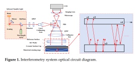
Semiconductor Wafer Flatness and Thickness Measurement Using Frequency Scanning Interferometry Technology​

State Key Laboratory of Precision Measuring Technology & Instruments.
Standard Optics Technology Tianjin Co., Ltd.,

Abstract​

Silicon (Si) and silicon carbide (SiC) are second- and third-generation semiconductor materials with excellent properties that are particularly suitable for applications in scenarios such as high temperature, high voltage, and high frequency. Si/SiC wafers face warpage and bending problems during production, which can seriously affect subsequent processing. Fast, accurate, and comprehensive detection of thickness, thickness variation, and flatness (including bow and warpage) of SiC and Si wafers is an industry-recognized challenge. Frequency scanning interferometry (FSI) can synchronize the upper and lower surfaces and thickness information of transparent parallel thin wafers, but it is still affected by multiple interfacial harmonic reflections, reflectivity asymmetry, and phase modulation uncertainty when measuring SiC thin wafers, which leads to thickness calculation errors and face reconstruction deviations. To this end, this paper proposes a high-precision facet reconstruction method for SiC/Si structures, which combines harmonic spectral domain decomposition, refractive index gradient constraints, and partitioning optimization strategy, and introduces interferometric signal “oversampling” and weighted fusion of multiple sets of data to effectively suppress higher-order harmonic interferences, and to enhance the accuracy of phase resolution. The multi-layer iterative optimization model further enhances the measurement accuracy and robustness of the system. The flatness measurement system constructed based on this method can realize the simultaneous acquisition of three-dimensional top and bottom surfaces on 6-inch Si/SiC wafers, and accurately reconstruct the key parameters, such as flatness, warpage, and thickness variation (TTV). A comparison with the Corning Tropel FlatMaster commercial system shows that this method has high consistency and good applicability.​

1751319609538.png

Please, Log in or Register to view URLs content!
 

gelgoog

Lieutenant General
Registered Member
Indeed until one year ago SMIC top 7nm wafers (and photoresist) were still from Japan, maybe also today they still buy top quality 12" wafers from Japan...

Nobody knows for how long this faucet will remain open for SMIC, hopefully they are not far from localizing the whole wafer supply chain and chemicals....
Japanese wafer vendor SUMCO were already complaining months back that they lost YMTC as a customer.
Please, Log in or Register to view URLs content!

So I think the Chinese wafers are already good enough for at least 28nm.
 

tphuang

General
Staff member
Super Moderator
VIP Professional
Registered Member
Please, Log in or Register to view URLs content!

CETC and Xiaohua Semi announced adaptation work for first domestic safety vehicle control software platform based on Xiaohu's XC27x series of chips have completed. Providing industry with full stack domestic automotive underlying tech solution from chips to software.

high temperature silicon furnace by CETC was successfully shipped. This indepdently developed SiC chemical vapors deposition equipment was successful. Equipment can smoothly achieve purity of coating products >= 99.9999% and thickness of coating is 100 micros.
 

european_guy

Junior Member
Registered Member

“China’s foundry production capacity is superior to Korea’s… No. 1 in the world in 5 years”​


Here another report from Yole Group (usually a reliable source) through a Korean news site:

Please, Log in or Register to view URLs content!

Market research firm Yole Group recently published a report on the current status of the semiconductor foundry industry, stating that China accounted for 21% of the world’s foundry production capacity last year. This is second only to Taiwan, which ranked first with 23%. Korea ranked third with 19%, followed by Japan (13%), the United States (10%), and Europe (8%).

1751359637094.png


Please note this is installed capacity (in wafers per months) not revenues nor actual production (fabs don't run at 100% capacity). Regarding revenues China has still some gap to fill against TSMC and Samsung.

But from an industrial ecosystem and supply chain POW capacity is more important, it is directly linked to number of fab lines, equipment, upstream materials and chemicals.

This report refers to 2024 data. IIRC it is the first time China is above Korea, in 2023 Korea was still Nr. 2
 

gelgoog

Lieutenant General
Registered Member
Yes. The PRC should be surpassing even Taiwan in wafer manufacturing capacity soon.

The problem is in terms of total transistors or gates the PRC will still be behind because of the lack of more modern tools.

Like I said before I expect China to become the world leader in DRAM, NAND, and "legacy" chips over the next decade. They don't require anything better than immersion lithography.

I think people still underestimate the future ramp up of capacity in China. Even with all those fab expansions being made, there is enough vacant land in those fab sites to double it again.
 

sunnymaxi

Major
Registered Member
Like I said before I expect China to become the world leader in DRAM, NAND, and "legacy" chips over the next decade. They don't require anything better than immersion lithography.
Lots of 7nm lines will come online by the end of this year and 5nm line by next year.. you will see China will also be the big player in FinFet chips by next decade.

Cambricon revenue jumped by 300% due to SMIC capacity allocation in 2025.

Image


Cambricon, Biren, Enflame, Moore Threads, MetaX They can finally get back on track now that SMIC 7nm allocation is available. AI chipmakers Moore Threads plans to raise $8B Yuan, while MetaX seeks $3.9B Yuan, according to their IPO filing.
 

gelgoog

Lieutenant General
Registered Member
Other than SMIC doubling its FinFET floor space are there any other such projects? The FinFET capacity still seems to be severely constrained to me. To be frank 5 years after 2020 sanctions I am surprised there is no evidence still that China surpassed the immersion lithography tool bottleneck.

I think SMIC needs to double its FinFET capacity again, and there needs to be a second player.
 
Last edited:

sunnymaxi

Major
Registered Member
Other than SMIC doubling its FinFET floor space are there any other such projects? The FinFET capacity still seems to be severely constrained to me. To be frank 5 years after 2020 sanctions I am surprised there is no evidence still that China surpassed the immersion lithography tool bottleneck.

I think SMIC needs to double its FinFET capacity again, and there needs to be a second player.
Two news i have heard.

1.Huawei is entering in FinFET. their fab is near completion.

2. Huahong could announce something related FinFet by next year.. they were planning but October, 2022 sanctions stopped.

and regarding Immersion lithography.

honestly, this is a top top secret. nobody is allowed to talk on this topic.. so we can only wait.
-------------------------------------------------------------------------------------------------------
remember, SiCarrier dropped the bombshell at SEMICON 2025. released all Non-Litho advance tools from 28nm to 5nm.

The presenter guy, clearly told we have a sweet surprise coming next year.

so i believe. we are very close to official announcement or solid hint regarding domestic immersion Lithography.
 
Top