Chinese semiconductor thread II

tokenanalyst

Brigadier
Registered Member

New heights of epitaxial equipment! NAURA compound epitaxial equipment leads the market boom​


Recently, two MOCVD (metal organic chemical vapor deposition) epitaxial equipment (models: Satur N800/Satur V700) independently developed by NAURA successfully passed the acceptance of leading customers in the industry and received batch repeat orders.

Since NAURA started the research and development of epitaxial equipment in 2010, after more than ten years of technological accumulation and innovative breakthroughs, it has achieved full coverage of 4-inch to 12-inch silicon thin film epitaxial equipment. Its products include 8-inch and below single-wafer and multi-wafer large-capacity silicon epitaxial equipment and 12-inch silicon epitaxial equipment. It has achieved many technological innovations and industrialization results, with cumulative sales exceeding 1,000 cavities. It has won the "Beijing Science and Technology Progress First Prize", the first "National Excellent Engineer Team", "Beijing Model Collective" and other heavyweight honors, becoming a leader in China's silicon thin film epitaxial equipment field.

Relying on its profound accumulation in the field of silicon epitaxial equipment, North Huachuang has actively expanded the research and development of compound semiconductor epitaxial equipment, and has formed a series of products of epitaxial equipment for compound semiconductor materials such as GaN (gallium nitride), GaAs (gallium arsenide), and SiC (silicon carbide).

1751399990081.png

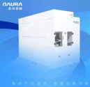
GaN MOCVD epitaxial equipment

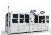
NAURA GaN MOCVD epitaxial equipment, Satur N800, is designed for the special needs of 8-inch silicon-based GaN power devices. It features a large-area uniform temperature field, a large-range stable and adjustable gas flow field, and multi-chip (Batch) large production capacity and automated configuration, which can meet the high requirements of compound semiconductor advanced devices for epitaxial layer composition, thickness and doping uniformity. At present, Satur N800 has entered many domestic compound semiconductor clients, successfully passed chip verification and stable operation, achieved batch shipments, and continuously received repeat orders.
1751400006765.png
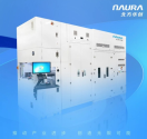
GaAs MOCVD epitaxial equipment

NAURA GaAs MOCVD epitaxial equipment, Satur V700, has successfully made breakthroughs in key technologies such as gas flow field, temperature field, and by-product control, and has the advantages of high uniformity, large production capacity, and low cost. This equipment can not only meet the pain point needs of the Micro LED industry, but can also be widely used in RF, optoelectronics and other fields. At present, Satur V700 has been shipped in batches to many customers and has passed strict chip verification. With its good performance, it continues to receive a large number of repeat orders from customers.
1751400027981.png

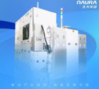
SiC epitaxial equipment

NAURA SiC epitaxial equipment, MARS iCE115/120S, features simple process debugging and convenient maintenance and operation, and quickly captured the market once it was launched. MARS iCE120S is compatible with 6/8-inch SiC epitaxy and has C2C capability, providing a good product choice for the market during the transition period when the SiC industry is shifting from 6-inch to 8-inch.
1751400047877.png

MARS iCE120S

As SiC epitaxial technology matures, NAURA has launched a multi-wafer 6/8-inch compatible SiC epitaxial product, Satur C960. The equipment uses a new independently developed temperature control architecture, vacuum exhaust system and multi-functional modular design, which can achieve 9 6-inch or 6 8-inch epitaxy in a single furnace. It has the advantages of high productivity, low cost and long uptime, further expanding the SiC epitaxial product market.

Please, Log in or Register to view URLs content!
 

tokenanalyst

Brigadier
Registered Member

Liande Equipment won the bid for BOE's 8.6th-generation AMOLED production line project and will supply automatic lamination machines

On June 30, Liande Equipment issued an announcement stating that the company recently received a "Notice of Winning Bid" from China Electronics Business (Beijing) Co., Ltd., confirming that the company has become the successful bidder for BOE's 8.6th generation AMOLED production line project. The winning equipment is an automatic lamination machine (D-lami) and the total bid amount is 157,273,400 yuan.
1751400434366.png

Liande Equipment stated that the implementation of this project will occupy a certain amount of the company's funds. If a formal contract is signed for this project and it is implemented smoothly, it will have a positive impact on the company's future operating performance.
Recently, BOE stated in an institutional survey that on May 20, the company's Chengdu 8.6-generation AMOLED production line project began to move in process equipment four months ahead of schedule, marking the transition of the production line from the construction phase to the production line operation phase, laying a solid foundation for subsequent product lighting and mass production delivery, and effectively promoting the global OLED display industry to accelerate its progress into the medium-size field.

At the same time, the 6th generation AMOLED production line in Mianyang (B11) and the 6th generation AMOLED production line in Chongqing (B12) have all completed the conversion.

Please, Log in or Register to view URLs content!
 

tokenanalyst

Brigadier
Registered Member

From January to May, China exported 135.9 billion integrated circuits, a year-on-year increase of 19.5%.​


Data show that from January to May, my country's electronic information manufacturing industry production grew rapidly, export growth slowed, efficiency improved steadily, investment growth fell, and the overall development trend of the industry was good.

According to the Industry and Information Technology Micro-News, from January to May, the added value of electronic information manufacturing industries above designated size increased by 11.1% year-on-year, 4.8 and 1.6 percentage points higher than the industrial and high-tech manufacturing industries in the same period, respectively. In May, the added value of electronic information manufacturing industries above designated size increased by 10.2% year-on-year. Among the main products, the output of mobile phones was 570 million units, a year-on-year decrease of 6.5%, of which the output of smart phones was 450 million units, a year-on-year decrease of 2.1%; the output of microcomputer equipment was 130 million units, a year-on-year increase of 5.5%; 193.5 billion pieces, a year-on-year increase of 6.8%.

In terms of exports, from January to May, the cumulative export delivery value of electronic information manufacturing industries above designated size increased by 3.3% year-on-year, down 1.2 percentage points from January to April. According to customs statistics, from January to May, my country exported 53.95 million laptops, down 2.9% year-on-year; exported 279 million mobile phones, down 7.7% year-on-year; and exported 135.9 billion integrated circuits, up 19.5% year-on-year.

In terms of efficiency, from January to May, the electronic information manufacturing industry above designated size achieved operating income of 6.49 trillion yuan, a year-on-year increase of 9.4%; operating costs of 5.7 trillion yuan, a year-on-year increase of 9.4%; total profits of 216.2 billion yuan, a year-on-year increase of 11.9%; operating income profit margin of 3.33%, an increase of 0.2 percentage points from January to April. In May, the operating income of the electronic information manufacturing industry above designated size was 1.37 trillion yuan, a year-on-year increase of 6.8%. In addition, from January to May, the fixed asset investment in the electronic information manufacturing industry increased by 7% year-on-year, down 2 percentage points from January to April, and 4.6 percentage points lower than the growth rate of industrial investment in the same period.

Please, Log in or Register to view URLs content!
 

tokenanalyst

Brigadier
Registered Member

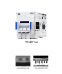
Shengmei Shanghai ECP equipment 1500 electroplating chamber successfully delivered.​


On June 30, the 1500 electroplating chamber of SCM Shanghai ECP equipment was successfully delivered, marking a breakthrough for SCM Shanghai in product iteration and upgrading and market expansion, and once again demonstrating the company's strength and influence in the industry.

1751473146370.png

The successful delivery of the ECP equipment 1500 electroplating chamber is a strong proof of the company's product strength. Shengmei Shanghai has always adhered to the differentiated independent innovation strategy, continuously increased R&D investment, and is committed to improving the technical level and performance indicators of its products. Through continuous technological innovation and product optimization, Shengmei Shanghai's electroplating equipment has won recognition and praise from customers in the market.

The ECP equipment 1500 electroplating chamber delivered this time has reached the industry-leading level in terms of stability, precision and efficiency, and can meet the diverse needs of customers in the semiconductor manufacturing process.

Please, Log in or Register to view URLs content!
 

tokenanalyst

Brigadier
Registered Member

With a total investment of 5.5 billion yuan, Xinde Technology's artificial intelligence advanced packaging and testing base project started​


The Xinde Technology Artificial Intelligence Advanced Packaging and Testing Base Project was officially started, with a total investment of 5.5 billion yuan.
The first phase of the project will invest 1 billion yuan, plan to build a 153,000 square meter modern plant, equip it with advanced production equipment, build two internationally leading high-end packaging production lines, and make every effort to overcome the packaging difficulties of AI computing chips, and accurately meet the high-performance packaging needs of 5G communications and automotive-grade chips. After the first phase is completed and reaches full production, it will be able to produce 18,000 2.5D packaged products and 300 million wafer-level high-density chip packaged products annually.

According to information, Jiangsu Xinde Semiconductor Technology Co., Ltd. was established in Pukou Economic Development Zone in September 2020. It is a high-tech enterprise focusing on semiconductor integrated circuit packaging and testing business. It has deployed high-end packaging products such as WLCSP, Bumping, LGA, BGA, 2.5D packaging, and successfully launched CAPiC grains and advanced packaging technology platforms. It has completed more than 2 billion yuan in financing and obtained financing support from multiple parties including Nan Venture Capital, Jinpu Fund, Xiaomi Industrial Fund, OPPO, Guoce Investment, and Kunqiao Capital.

Please, Log in or Register to view URLs content!
 

tokenanalyst

Brigadier
Registered Member

Semiconductor parts manufacturer Zhenbao Technology's IPO accepted​


The IPO application of Chongqing Zhenbao Technology Co., Ltd. (hereinafter referred to as "Zhenbao Technology") on the Science and Technology Innovation Board was recently accepted by the Shanghai Stock Exchange, and the guidance institution is CITIC Securities.
Zhenbao Technology is one of the few companies in China that has achieved multi-category supply and large-scale mass production of non-metallic components for advanced integrated circuit process equipment and high-generation, high-voltage display panel manufacturing equipment.
In this IPO, Zhenbao Technology plans to raise 1.398 billion yuan, of which 752 million yuan will be used for semiconductor and pan-semiconductor precision parts and materials production base projects, 282 million yuan will be used for Zhenbao Technology R&D center construction projects, 164 million yuan will be used for Shanghai Zhenbao Semiconductor Equipment Parts R&D Center projects, and 200 million yuan will be used to supplement working capital.

ICP and display panel component manufacturers
Zhenbao Technology focuses on providing integrated circuit and display panel industry customers with parts and surface treatment solutions for the parts involved in process reactions in the vacuum chamber of manufacturing equipment. The company's main products include equipment parts such as silicon, quartz, silicon carbide and alumina ceramics , as well as surface treatment services such as spray regeneration, anodizing and precision cleaning.
In terms of component products, Zhenbao Technology has mass-produced core components such as curved silicon upper electrodes, quartz gas distribution plates, and high-purity silicon carbide rings, and has supplied them in batches in the fields of logic-type 14nm and below technology node advanced process integrated circuit manufacturing, storage-type 200-layer and above stacked advanced process 3D NAND flash memory chip manufacturing, and 20nm and below technology node DRAM advanced process memory chip manufacturing.
In terms of raw material manufacturing, the company has mass-produced large-diameter single-crystal silicon rods for the production of silicon components, chemical vapor deposited silicon carbide materials for the production of high-purity silicon carbide components, and alumina and yttrium oxide ceramic granulated powders for the production of ceramic components, and continues to promote the iterative development of high-density ceramic coating preparation processes.
In terms of surface treatment, in the field of integrated circuit manufacturing, its surface treatment services have been supplied to the manufacturing of advanced process integrated circuits with technology nodes of 14nm and below for logic and advanced process 3D NAND flash memory chips with 200 layers and above for storage; in the field of display panels, it is supplied to high-end process production lines of display panels such as G10.5-G11 ultra-large generations and AMOLED.

Please, Log in or Register to view URLs content!
 

tokenanalyst

Brigadier
Registered Member
Lol. What to think of this piece ??
Couldn't be a more totally dif


This piece has a totally different take. Lol


It saying China fab equipments are idle because lack of maintenance and support from foreign suppliers.
That i sjust an slop Youtube, probably AI ChatGPT bot generated crap because the stooge is to lazy to earn his money doing basic google search research.
 

GulfLander

Colonel
Registered Member
US Lifts Chip Design Curbs On China as Part of Trade Deal
The Trump administration has lifted export license requirements for chip design software sales in China.
The US Commerce Department informed leading chip design software providers that they no longer need government licenses to do business in China.
The move is part of a trade deal in which Washington will allow shipments of chip-design software to China, and Beijing will speed approval of critical mineral exports.
Please, Log in or Register to view URLs content!

Please, Log in or Register to view URLs content!
 
Top