Chinese semiconductor thread II

tokenanalyst

Brigadier
Registered Member

Comparison Measurements of Natural Constants Based on Laser-Focused Atomic Deposition and Extreme Ultraviolet Interference Lithography.​

Abstract​

Traceability is the foundation of accuracy and consistency in dimensional metrology. Meter in the International System of Units is defined and reproduced by natural constants, and comparing the differences in traceability approaches based on different natural constants can better understand the real size of manufacturing structures. This paper compares the consistency of three traceability approaches based on chromium atomic transition wavelength, iodine-stabilized laser wavelength (top-down approach), and silicon lattice spacing (bottom-up approach) in nanoscale dimensional metrology. The measured objects for comparison are silicon gratings manufactured by laser focused atomic deposition (LFAD) and extreme ultraviolet interference lithography (EUV IL), and the pitch of the silicon gratings can be traceable to the transition wavelength of chromium (7S3→7P4, lambda=425.5533 nm). For the silicon grating manufactured by LFAD and EUV IL at diffraction order m=1, the expected pitch of the silicon grating is lambda/4. The pitch of the silicon grating is measured using top-down (metrological AFM) approach, and the deviation between the measured result and the pitch based on the transition wavelength of chromium is 0.1 nm. For the silicon grating manufactured by LFAD and EUV IL at diffraction order m=2, the expected pitch of the silicon grating is lambda/8. This silicon grating is measured using bottom-up approach, and the deviation between the measured result and the pitch based on the transition wavelength of chromium is 0.2 nm. This research provides a feasible solution for integrating various measurement methods or different traceability approaches at nanoscale, and demonstrating the potential and feasibility of a nanoscale dimensional metrology traceability chain based on self-traceable gratings.

Please, Log in or Register to view URLs content!
 

tokenanalyst

Brigadier
Registered Member

KingSemi: Multi-category core components are gradually being replaced by domestic products​

A relevant person in charge of Xinyuan Micro responded to the Securities Times reporter about the impact of the "Entity List" and said that Xinyuan Micro attaches great importance to the R&D verification and independent control of core components, and actively supports the introduction of domestic component products. Core components such as manipulators, hot plates, photoresist pumps, etc. are gradually being replaced by domestic products. At present, the company's production and operation are all normal, and various businesses are progressing steadily. The overall impact of being included in the Entity List is controllable and will not have a substantial impact on the company's operations.​

Please, Log in or Register to view URLs content!
 

tokenanalyst

Brigadier
Registered Member

Keep pace with the times and lead the future! Oriental Crystal Source Computational Lithography PanGen V5.0 is coming​


OPC (Optical Proximity Correction) is a lithography resolution enhancement technology that compensates for image distortion caused by diffraction-limited imaging by correcting the pattern on the mask, thereby improving the yield in the chip manufacturing process. Since its establishment in 2014, Dongfang Jingyuan has creatively proposed a full-chip inverse lithography technology (ILT) computational lithography solution based on a CPU+GPU hybrid computing architecture, and based on this, formed the PanGen® yield comprehensive optimization product. After 10 years of development and iteration, this product has been widely used in the process research and development and mass production of mainstream domestic logic and storage chip manufacturers.
Product Introduction
In November 2024, Oriental Jingyuan launched PanGen® V5.0 to meet the needs of domestic cutting-edge customers. The main features and functions of this product include:
1. Continuing the idea of full-chip reverse lithography technology, we launched ILT solutions that meet different mask complexities, including Freeform Sbar, Freeform mask, and curvelinear mask. The Manhattan-based Freeform mask solution has been verified in silicon wafers in advanced node manufacturing, and the results show that the lithography process window for hole-shaped layouts can be increased by more than 20%.
1733346173822.png
2. Fully supports mainstream x86, NVIDIA GPU computing cluster ecosystems, as well as domestic computing clusters such as ARM computing clusters and Haiguang DCU. At the same time, PanGen® V5.0 supports cloud services and cloud computing.
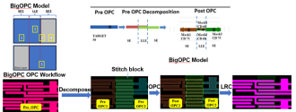
3. To meet the needs of large-area OPC in advanced packaging processes, PanGen BigOPC® products support multi-mask splicing exposure technology.
4. In response to the needs of silicon photonic device manufacturing process simulation optimization, PanGen® V5.0 supports the processing of multiple curved layouts and can check the mask optimization and lithography rules of any curved graphics.At the same time, considering the difference in requirements between silicon photonic devices and traditional chips, a curve target layout mask optimization function has been specially developed and has been verified by customers.
5. For high-end chip manufacturing, the long-range loading effect of etching is one of the main factors affecting the wafer mass production yield. To this end, PanGen® V5.0 has developed an AI-based etching model and etching automatic compensation mechanism, which can effectively predict the long-range loading effect and automatically calculate the etching compensation amount, thereby enhancing the consistency of the pattern and effectively improving the customer's overall yield.
Outlook
Dongfang Jingyuan will continue to be deeply rooted in the soil of customer needs, continue to deepen technological innovation, continue product iteration research and development, continuously expand product line coverage, continuously improve product functions, continuously improve product performance, actively implement HPO (Holistic Process Optimization) yield maximization technology route and product design concept, and strive to create the GoldenFlow of China's chip manufacturing. Effectively solve customers' technical problems in the chip manufacturing process, provide customers with computational lithography solutions that keep pace with the times, and create value for customers!

Please, Log in or Register to view URLs content!
 

tokenanalyst

Brigadier
Registered Member

Photo-emission electron gun and electron optical simulation for ultrafast scanning electron microscope​


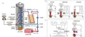
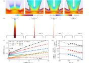
Ultrafast scanning electron microscope (USEM) integrates pump-probe technique with microscopic imaging, enabling the visualizing of photon-induced surface charge dynamics with high spatial and temporal resolution. This capability is crucial for high-resolution detection of semiconductor surface states and optoelectronic devices. This work discusses the parametric design of a thermionic emission electron gun that has been modified into a photoemission electron gun, based on a home-built ultrafast scanning electron microscope. Given that the dose of the photoemitting electron beam is usually much lower than that of thermal emission, the transition to photoemission requires the removal of the self-bias voltage function of the original electron microscope power supply to ensure the normal operation of the Wehnelt electrode. We quantitatively analyze the dependence of bias voltage, cathode, Wehnelt electrode , and anode on the position, size and divergence angle of crossover, which helps to improve the parameter adjustment of the modified electron gun. The analysis results indicate that if the distance between the Wehnelt electrode and the anode is adjusted from 8 to 23 mm, the distance between the filament and wehnelt can be changes from 0.65 to 0.45 mm to cooperate with the bias adjustment, so that the normal use of high-resolution thermionic emission mode, low voltage mode and photoemission mode can be realized. Subsequently, the effect of the mirror's position on the electron optical path is analyzed. It is found that when the anode is raised 1.4 mm above the mirror, the influence on the electron optical path can be ignored. Additionally, the zero-of-time and temporal broadening of the photo-electron pulse are further simulated. The results indicate that with the increase of bias voltage, the time zero of photoemission will be delayed and the temporal broadening will become larger. This study lays a foundation for the future development of ultrafast electron microscope and the design of photoemission electron sources.​


1733347465640.png
1733347488910.png

Please, Log in or Register to view URLs content!
 

tokenanalyst

Brigadier
Registered Member

The new production center of Ruili Scientific Instruments was officially put into use, opening a new chapter in mass testing​


Recently, Ruili Scientific Instruments (Shanghai) Co., Ltd. held a launching ceremony for its new production center. The company's latest optical measurement equipment TFX-R3 and optical defect detection equipment BriteSD300 were launched at the launching ceremony. This event marks Ruili's entry into a new stage in the field of semiconductor measurement and testing, and has injected strong momentum into the company's future development.

1733352931846.png

With the rapid expansion of business scale, especially the sharp increase in order volume, Ruili Scientific Instruments (Shanghai) Co., Ltd.'s original clean production site in Heqing has reached saturation. In order to meet this challenge and meet new development needs, the company decided to expand a new production base in Gubo Road Science Park.

In this golden autumn season, the new production center with a total area of 4,000 square meters was officially put into use. Among them, the Class 1,000 clean workshop occupies half of the area, reaching 2,000 square meters. The commissioning of this new center is not only a powerful supplement to the company's current production capacity, but also provides a solid backing for future business growth.

The establishment of the new production center is an important measure for Ruili Scientific Instruments to actively adjust its strategy and expand its production capacity in the face of market challenges. It will greatly enhance the company's production capacity and service quality, ensuring that the company can continue to provide customers with high-quality products and services. The completion of this new position marks that Ruili Scientific Instruments has stepped onto a new level in the field of integrated circuit measurement.

Please, Log in or Register to view URLs content!
 

cctang

New Member
Registered Member
Please, Log in or Register to view URLs content!


Another guess as to what's happening with 9020, I think roughly in line with my speculation. Some process improvement on the core chips, but larger breakthrough on a chiplet design that helps dramatically improve power efficiency.

The Kirin 9020 has made unexpected progress, with chiplet stacking and advanced packaging showing initial power #Mate70KirinChipFirstTeardown#
Some friends have already gotten their hands on the Mate70 Pro+ device. Some media outlets have disassembled it, measured the chip size, and evaluated its performance. I was shocked to find that the core chip, Kirin 9020, has made significant progress compared to the Kirin 9000S in the Mate60 Pro. It's expected that when foreign media like TechInsights get the device and cut open the chip for measurement, they will reveal new microscopic discoveries.
Why did I intuitively think the progress wouldn't be too significant? Because it uses DUV lithography for manufacturing, which is obviously much more complicated than EUV lithography and severely limited. It was already challenging to produce the 7nm Kirin 9000S, so it seemed difficult for the Kirin 9020 to make a big leap in performance. I expected small chip improvements but major system-wide advancements in AI, heat dissipation, pure HarmonyOS, etc. The launch event didn't discuss the chip, keeping it mysterious.
However, the Kirin 9020 is truly exceptional. Compared to the 9000S, it's visibly larger in area and notably thicker. The area is 14.5mm16.25mm, clearly larger than the 9000S's 14.614.26, an increase of 14%. The thickness is 0.58mm compared to 0.42mm. I personally guess that the FINFET process platform for chip manufacturing has improved, increasing the number of transistors per unit area, and the device design has changed, making transistors more "three-dimensional".
The FINFET process principle involves growing dense silicon needle-like hairs called fins on a silicon base. Then metal rings called gates encircle each fin. The shape of these fins has become more slender, making them more sensitive to gate control voltage, reducing power consumption, and effectively progressing from 7nm to 5nm equivalent. This is all my speculation, but within expectations.
What's unexpected is that it's become much thicker, likely due to the use of chiplet "chip stacking" and advanced packaging technology. This is impressive, essentially turning a 2D chip into 3D, increasing transistor count in another dimension. Specific details are unknown, but this opens up future development possibilities. We need to strengthen learning in this area, which belongs to advanced packaging technology. It's different from chip manufacturing processes but can significantly enhance chip performance.
The overall effect is that many functions are now integrated into the Kirin 9020. Communication baseband, satellite communication, CPU, NPU neural network computing, GPU, storage, ISP imaging algorithms are distributed among several chiplets, then connected using advanced packaging in planar and vertical arrangements. If it's vertical connection, it's called "chip stacking" in 3D or 2.5D. The connecting lines are very thin and dense, beyond the capabilities of general packaging, requiring advanced packaging. It's less difficult than wafer processing but still challenging. TSMC excels at this. They might have set up an advanced packaging production line within their capabilities.
The integration effect is impressive, with the chip being quite advanced, able to run 6 large games simultaneously without lag. Power consumption is low, with one comparative test showing the Kirin 9020's whole device power consumption at 0.69W, while the Snapdragon 8 Gen 3's was 0.94W. It can run TikTok for 14 hours continuously without overheating and with sufficient battery life.
I guess (all technical information is speculation except for user-tested data) that the Kirin series has found a way to develop continuously, mainly relying on advanced packaging and chip stacking for 3D development. Chip manufacturing processes are still challenging, with 5nm being very limiting. It's said that with persistence, DUV lithography could push to 3nm. But with chiplet technology and chip architecture improvements, overall performance can keep up, performing like a 4nm chip. Currently, production capacity is limited, but advanced chip performance won't be completely stalled.
 

tphuang

General
Staff member
Super Moderator
VIP Professional
Registered Member
Please, Log in or Register to view URLs content!


Another guess as to what's happening with 9020, I think roughly in line with my speculation. Some process improvement on the core chips, but larger breakthrough on a chiplet design that helps dramatically improve power efficiency.
this kind of stuff goes without question. Every year, Mediatek and QCOM also improve their chip through design improvement. This is nothing new.
 

Hyper

Junior Member
Registered Member
Please, Log in or Register to view URLs content!


Another guess as to what's happening with 9020, I think roughly in line with my speculation. Some process improvement on the core chips, but larger breakthrough on a chiplet design that helps dramatically improve power efficiency.
Chiplets have higher ideal power consumption than monolithic dies. Let's wait for techinsights teardown.
 

tokenanalyst

Brigadier
Registered Member

Unisoc wearable chip matrix continues to enrich and lead the new stage of 5G development​


With the rapid advancement of technology and the changing consumer demand for wearable products, the market is undergoing unprecedented changes. According to the latest data from Canalys, in the second quarter of 2024, the global wearable wristband device market shipments will stabilize at around 44 million units. This figure not only highlights the huge potential of the market, but also indicates the unlimited possibilities of wearable technology in the future.
The development of the smart wearable industry is inseparable from the support of the underlying chips. In 2024, well-known brands such as vivo, Xiaomi, and Honor have successively released a new generation of smart watches, among which the W117 chip equipped with UNISOC has made an indelible contribution. With its excellent performance and wide application, it has become the new favorite of smart wearable devices. Looking at the development history of UNISOC's smart wearable product business, it is not difficult to find that as the product matrix continues to be enriched and improved, and the product strength is constantly recognized by first-line brand manufacturers, its important leadership position in the field of smart wearables is becoming increasingly prominent.

Please, Log in or Register to view URLs content!
 
Top