Chinese semiconductor thread II

tokenanalyst

Brigadier
Registered Member

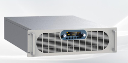
The United States has increased its control over semiconductors in China, and domestic substitution of RF power supplies has accelerated​


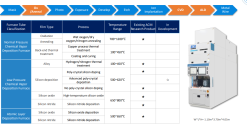
U.S. sanctions on technology blockades have promoted the accelerated verification of domestic RF power supplies. The replacement of RF power supplies has a great impact on the process. Customers have previously had little willingness to replace, but the "semiconductor manufacturing" end-use restrictions introduced by the United States in October 2022 further restricted the development of domestic semiconductors. RF power supplies have become one of the "neck" links, and the demand for domestic substitution is urgent. Domestic equipment companies are facing an increasingly close risk of supply interruption, prompting equipment-end customers to accelerate domestic substitution. RF power supply is one of the semiconductor equipment components with high technical barriers. To achieve high power and high efficiency, manufacturers need to have a deep technical accumulation of internal circuit and structural design, and cooperate with customers to continuously debug.​

1733266129034.png
 

tokenanalyst

Brigadier
Registered Member

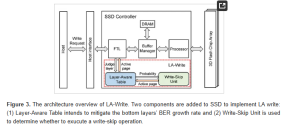
Balancing Page Endurance Variation Between Layers to Extend 3D NAND Flash Memory Lifetime​

Abstract​

With vertical stacking, 3D NAND’s flash memory can achieve continuous capacity growth. However, the endurance variation between the stacked layers becomes more and more significant due to process variation, which will lead to the underutilization of many pages and seriously affect the lifetime of 3D NAND’s flash memory. We investigated the endurance variation characteristics between layers and divided the stacked layers into the top, middle, and bottom layers according to the endurance characteristics. We found that the endurance of the bottom layer pages is much weaker than that of the other two layers, which is the primary factor that affects the lifetime of 3D NAND’s flash memory. In response to this endurance variation feature, we proposed a new layer-aware write strategy, called LA-Write. First of all, the write–skip unit in LA-Write will reduce the wear pressure of the pages through write–skip operations. Secondly, LA-Write maintains a layer-aware table, which stores the probability of pages in different layers performing the write–skip operation. Setting the probability of the bottom pages to the highest value will result in more write–skip operations on the bottom layers, mitigating endurance variations between layers. We carried out our experiments of LA-Write on DiskSim, a popular SSD simulator. Compared to existing schemes, experimental results show that LA-Write can greatly increase SSD’s lifetime.​

1733266280091.png

Please, Log in or Register to view URLs content!
 

cctang

New Member
Registered Member
Any more news / speculation / discussion about the possibility that the HW 9020 SOC is dependent on advanced packaging / chiplet, to increase transistor count without sacrificing yield? Super interesting development if true.

We always knew this was a possibility, but if it really translated into 30%+ increase in performance, significant reduction in heat... all at the "cost" of a few square mm of real estate on the PCB... that's a game changer.
 

JPaladin32

New Member
Registered Member
little.jpgmid.jpgbig.jpg
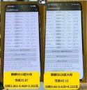
A preview of Kirin 9020 performance and efficiency. Quite insane improvements on little and mid cores. 60% higher score at roughly the same power on littles, 6% higher score at 20% less power on mids. Not much efficiency change on the big core. Improved performance on the big but also higher power.

I'm quite confused by these numbers. You'd think the huge efficiency jump on littles and mids indicates a massively improved lithography process. Before seeing the big core I'd even conclude this is 5nm. But then the big core efficiency hasn't changed, so there is the chance that the litho process hasn't improved much but HiSilicon pulled something magical.
 

cctang

New Member
Registered Member
Just speculating here - what about the possibility the smaller cores are on 5nm chiplet (where yield is less of an issue because of size), the large core is on the same 6nm, and they're all just packaged together?
 

Hyper

Junior Member
Registered Member
View attachment 140379View attachment 140380View attachment 140381
A preview of Kirin 9020 performance and efficiency. Quite insane improvements on little and mid cores. 60% higher score at roughly the same power on littles, 6% higher score at 20% less power on mids. Not much efficiency change on the big core. Improved performance on the big but also higher power.

I'm quite confused by these numbers. You'd think the huge efficiency jump on littles and mids indicates a massively improved lithography process. Before seeing the big core I'd even conclude this is 5nm. But then the big core efficiency hasn't changed, so there is the chance that the litho process hasn't improved much but HiSilicon pulled something magical.
Probably a more optimised process. Kirin 9000 was not good.
 

Proton

Junior Member
Registered Member
View attachment 140379View attachment 140380View attachment 140381
A preview of Kirin 9020 performance and efficiency. Quite insane improvements on little and mid cores. 60% higher score at roughly the same power on littles, 6% higher score at 20% less power on mids. Not much efficiency change on the big core. Improved performance on the big but also higher power.

I'm quite confused by these numbers. You'd think the huge efficiency jump on littles and mids indicates a massively improved lithography process. Before seeing the big core I'd even conclude this is 5nm. But then the big core efficiency hasn't changed, so there is the chance that the litho process hasn't improved much but HiSilicon pulled something magical.
Could it be about increasing yields on a new node?
By increasing voltage on mid cores, and even more on big cores, a bigger percentage of chips might make the cutoff?
 

tokenanalyst

Brigadier
Registered Member

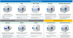
Semiconductor equipment and components manufacturer Torrance completes Series A+ financing​


Torrance Precision Manufacturing (Jiangsu) Co., Ltd. announced the completion of its A+ round of financing. The investor is Shenyang Chengtai Investment Management Co., Ltd. The specific financing scale has not yet been disclosed. This investment is an important progress in Torrance Equipment's capital operation, which will help the company further expand its market, enhance its technical strength and production capacity. As an investor, Shenyang Chengtai Investment Management will provide support to Torrance Equipment in terms of capital, resources, management, etc., to help the company develop rapidly.

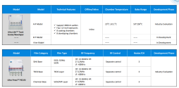
Torrance Equipment was founded in September 2004 and is headquartered in Shanghai. It is a professional high-end equipment OEM supplier. The company's main products cover the key links of semiconductor equipment integrated circuit manufacturing, including etching, thin film deposition, photolithography and coating development, chemical mechanical polishing, ion implantation, etc. The company relies on its professional capabilities and technical accumulation in these fields to provide customers with high-quality products and services.

In the field of semiconductor equipment parts, Torrance Equipment has significant technical advantages and market competitiveness. With the completion of this round of A+ round of financing, the company will further strengthen innovation and development in this field to meet the growing market demand. Through continuous technological innovation and product upgrades, Torrance Equipment is committed to becoming a leading company in the field of semiconductor equipment parts.

1733322668541.png

Please, Log in or Register to view URLs content!
 

LanceD23

Junior Member
Registered Member
After the 4 large associations in China publically announced US chips are Not safe to use.


The car chip association quickly announced the white list with 1800 domestic chips substitution.
Looks like they are preparing this action for while, just waiting for US to make the move first and then counter strike and pushing out its domestic substitutions.
Targeting US Texas Instrument, Analog Device, Onsemi, Microchip...

Hopefully the other 3 association will present their own similar lists.


Please, Log in or Register to view URLs content!


本次进入白名单的产品覆盖了车身、底盘、动力、座舱、智驾、整车控制等各应用领域中应用的10大类芯片。其中,电源类、通信类和控制类芯片型号数量最多,供应商也最广泛,这几类芯片在车上需求量大款型多,大部分性能需求不高,为国产芯片上车提供了广阔的市场空间。
1733335378480.png
 
Last edited:
Top