Chinese semiconductor thread II

tokenanalyst

Brigadier
Registered Member

With a total investment of 5 billion yuan, the AiSi Technology Park Packaging and Testing Project officially broke ground​


AiSi Technology Park has a total investment of 5 billion yuan, covers an area of 121 mu, has a construction area of about 200,000 square meters, and is equipped with high-rise factories, comprehensive supporting buildings, semiconductor professional factories and related supporting facilities. As the base camp of AiSi Technology, the project will build a headquarters, four manufacturing bases, and two R&D centers. At the same time, it will introduce semiconductor advanced equipment industry, semiconductor material cutting-edge R&D companies, and chip system integration and sales projects to create a semiconductor packaging and testing industry chain park supported by R&D.

AiSi Technology spans the two fields of "design" and "packaging and testing" in the semiconductor chip industry. In the field of packaging and testing, the existing Xuzhou packaging plant mainly uses wire bonding packaging forms such as SOP/SOT, QFN, DFN, high-end SIP system-level packaging, and wafer-level packaging such as WLCSP as the main packaging forms. In December 2022, "Anhui AiSi Semiconductor Co., Ltd." was established in Fuyang, Anhui as a professional testing plant. In February 2023, "Anhui AiSi Semiconductor Co., Ltd."

Please, Log in or Register to view URLs content!
 

tokenanalyst

Brigadier
Registered Member
Chuzhou Huarui Microelectronics Technology Co., Ltd. recently obtained a patent called "An ion implanter for integrated circuit production lines", with the authorization announcement number CN117594405B, the authorization announcement date is May 17, 2024, and the application date is November 20, 2023.
1716819415004.png


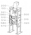
The present application discloses an ion implanter for an integrated circuit production line, which relates to the technical field of semiconductor processing equipment, and comprises a support frame, an ion implantation mechanism, an irradiation box assembly, a spoiler mechanism, and also a dust suction and dust removal assembly. By optimizing and improving the structure of the irradiation box assembly of the ion implanter in the prior art, a dust suction and dust removal assembly is added therein, and an elastic film coated with a self-adhesive adhesive is used in conjunction with the spoiler mechanism to absorb dust scattered in the box. The technical effect is achieved that when the ion implanter for an integrated circuit production line processes a circuit board, there are fewer particles in the irradiation box and it is not easy to invade the irradiation path of the ions.

Please, Log in or Register to view URLs content!
 

tokenanalyst

Brigadier
Registered Member

Composite semiconductor wafers company​

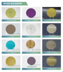
Building a new semiconductor material supply system: Pioneer in composite substrate materials - Qinghe Jingyuan, independently developed SiC composite substrate Emerald-SiC®​


With the rapid development of global science and technology, the importance of chips is self-evident, and one of the core technologies supporting all of this is semiconductor substrate materials . As one of the few semiconductor companies in the world that has mastered a full set of advanced semiconductor materials and heterogeneous integration technologies, Qinghe Jingyuan has set a new benchmark for the industry in the field of composite semiconductor substrate materials .

Qinghe has always been committed to the research and development of high-performance and low-cost composite substrate materials . It was the first to put into operation the first advanced semiconductor composite substrate production line in China and successfully developed SiC composite substrates through independent intellectual property rights.Emerald-SiC ® At the same time, the company is committed to high-quality and multi-faceted product development, and has successfully developed a variety of 6-inch and 8-inch homogeneous and heterogeneous composite substrate materials, such as: conductive SiC composite substrates, semi-insulating SiC composite substrates, SOI substrates, LN on Si composite substrates, LT on Si composite substrates, Si on ALN composite substrates, LT on Quartz composite substrates, etc., and has the foundation for large-scale mass production.

1716820408690.png

Please, Log in or Register to view URLs content!
 

tokenanalyst

Brigadier
Registered Member
Tongcheng New Materials getting in semiconductor CMP pads,this material is dominated by dupont​

Invest 300 million yuan! Tongcheng New Materials' subsidiary signs semiconductor chip polishing pad project in Jintan.​


Tongcheng New Materials' wholly-owned subsidiary Shanghai Tongcheng Electronic Materials Co., Ltd. signed the "Semiconductor Chip Advanced Polishing Pad Project" Cooperation Agreement with the Management Committee of Jiangsu Jintan Hua Luogeng High-tech Industrial Development Zone.

The "Semiconductor Chip Advanced Polishing Pad Project" has a registered investment of 300 million yuan. It plans to build a new semiconductor chip polishing pad production base in the Hua Luogeng High-tech Zone, mainly engaged in the research and development, production and sales of semiconductor chip polishing pads. After the project is successfully put into production, it can achieve an annual output of 250,000 semiconductor chip advanced polishing pads and an estimated annual sales of approximately 800 million yuan.

Please, Log in or Register to view URLs content!
 

tokenanalyst

Brigadier
Registered Member

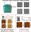
High efficiency polishing of micro-structured NiP alloy using isotropic electrochemical etching for achieving sub-nanometer roughness.​

Abstract​

Electroless plated nickel phosphorus (NiP) alloy is an essential engineered material used in optical applications, particularly in the field of extreme ultraviolet (EUV) technology, where high reflectivity of short-wavelength light is required. However, it is still challenging to achieve highly efficient sub-nanometer polishing of NiP plating, especially for micro-structured NiP surface. This study introduces isotropic etching polishing (IEP) as a novel ultra-precision processing technique for NiP plating, which is a damage-free and quick metal polishing technology through the amalgamation of contiguous etching pits. IEP was performed for 4 mins, leading to the attainment of a sub-nanometer surface exhibiting a Sa roughness of 0.065 nm, which verified efficiency and feasibility of the method. The IEP of NiP plating under various applied voltages is categorized into three stages: the etching stage, the limited current plateau stage, and the gas evolution stage. Experimental results bear witness to the direct correlation between the material removal rate (MRR) and surface roughness of NiP plating, specifically in relation to the sulfuric acid content within various electrolyte ratios. The most efficacious electrolyte composition was found to be 5:100 (H2SO4:CH3OH). Furthermore, the technology achieved ultra-smooth and shape-preserving polishing with a surface roughness below 0.1 nm, as confirmed by the comparisons of both the grating microstructure and Fresnel lens before and after IEP. The findings presented in this study are highly valuable for comprehending the process development and viability of IEP for NiP plating.

1716846624627.png

Please, Log in or Register to view URLs content!
 

tokenanalyst

Brigadier
Registered Member

193 nm immersion photodetector with an ultra-high EQE of 83.7%.​

Abstract​

With the development of chip to high-density integration, the requirement of lithography precision is higher and higher. In this process, controlling the power of the lithography exposure light source is very important to improve the quality of the chip. However, most detectors are unable to conduct light detection in liquid environments, especially in the aspects of real-time detection and calibration of light power in immersion deep ultraviolet lithography. In this paper, the AlN film epitaxial on n-SiC substrate by MOCVD is used as the photoelectrode, based on which an immersion detector with a quick response to 193 nm vacuum ultraviolet (VUV) light is fabricated. Impressively, under 0 V bias, the detector achieves a high responsiveness (130 mA/W) and an EQE up to 83.7% under an excitation with lower light power (45 nW), illustrating its ability to perform highly efficient detection of light signals and underwater imaging in weak-light environment. In addition, the detector also has the shortest detection wavelength when compared with the immersion photodetectors reported so far. At the same time, the simulated immersion lithography monitoring experiment shows that the detector has good real-time monitoring ability. In a word, this work provides a novel method for detecting underwater light power and can work as reference for realizing the real-time monitoring of immersive lithography light sources in future applications.

Please, Log in or Register to view URLs content!
 

measuredingabens

Junior Member
Registered Member
Please, Log in or Register to view URLs content!

Yttrium-doping-induced metallization of molybdenum disulfide for ohmic contacts in two-dimensional transistors​


Abstract​

The van der Waals systems could be used to overcome the issue of Fermi-level pinning in contacts of transistors based on two-dimensional semiconductors. However, the lack of advanced-node-lithography-compatible methods limits the use of such materials in wafer-scale integrated manufacturing. Here we report a yttrium-doping approach to convert semiconducting molybdenum disulfide (MoS2) into metallic MoS2. The approach, which is compatible with advanced-node wafer-scale integration, improves the band alignment and provides ohmic device contacts. It is based on a solid-state-source three-step doping method involving plasma, deposition and annealing, and can provide ångström-thickness surface doping. The yttrium-doped MoS2 acts as a metallic buffer that improves charge carrier transfer from the metal electrode to semiconducting MoS2. With this approach, we fabricate self-aligned, 10-nm-channel-length MoS2 field-effect transistors on two-inch wafers with an average contact resistances of 69 Ω µm and total resistances of 235 Ω µm. Our devices exhibit an ON-current density of 1.22 mA µm–1 at a drain voltage of 0.7 V, a ballistic ratio of 79% and a transconductance of 3.2 mS µm–1.
 

Michael90

Junior Member
Registered Member
BYD Semiconductor made a presentation today of its chip portfolio. It claims to have chips that cover 80% of all auto grade chips. Now, even if the actual % is lower than that, you can see the 10% self sufficiency claims by Nikkei are complete nonsense

Seems BYD has always been about self sufficiency and control of her supply chains than relying on others for her critical equipment. Think one of the only major Chinese company to have had such a policy long before any US sanctions ? Seems they are reaping the rewards which also translate to more efficiency and ease costs.
 

tokenanalyst

Brigadier
Registered Member

New ALD Tungsten tool from AMEC​

Diversified growth momentum is strong, and new thin film equipment products of AMEC are launched one after another​


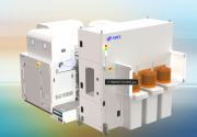
Recently, AMEC (Shanghai) Co., Ltd. (hereinafter referred to as "AMEC", stock code: 688012) launched its independently developed 12-inch high aspect ratio metal tungsten deposition equipment Preforma Uniflex ® HW and 12-inch atomic layer metal tungsten deposition equipment Preforma Uniflex ® AW. This is a cost-effective and high-performance solution provided by AMEC for ultra-high aspect ratio and complex structure metal tungsten filling in various device chips after Preforma Uniflex ® CW. AMEC has been deeply engaged in the field of high-end micro-processing equipment for many years and has continued to increase its investment in innovation and research and development. The launch of a number of new products this time is a new breakthrough for the company in the field of semiconductor thin film deposition equipment, and also provides strong growth momentum for the company's diversified business development.

The 12-inch Preforma Uniflex® HW equipment independently developed by AMEC with ultra-high aspect ratio filling capability inherits the advantages of the previous generation Preforma Uniflex® CW equipment and can be flexibly configured with up to five dual-stage reaction chambers. Each reaction chamber can process two wafers at the same time, while ensuring low production costs and achieving high production efficiency. Preforma Uniflex® HW adopts a growth gradient inhibition process with completely independent intellectual property rights, which can achieve precise process control from passivation-dominated to etching-dominated on the surface. In terms of hardware, the control system developed by AMEC can achieve passivation time from milliseconds to thousands of seconds, which can meet the filling of a variety of complex structures. In addition, with the optimized flow field thermal field system, the equipment has excellent film uniformity and process adjustment flexibility.

1716906686870.png


Please, Log in or Register to view URLs content!
 
Top