Chinese semiconductor thread II

GulfLander

New Member
Registered Member
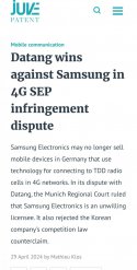
Datang wins against Samsung in 4G SEP infringement dispute - juvepatent
Screenshot_20240429_234956_Chrome.jpg
"Samsung Electronics has infringed
Please, Log in or Register to view URLs content!
, owned by Datang Mobile Communications Equipment, and currently may not sell 4G-capable mobile devices in Germany. The Munich Regional Court handed down this decision in mid-April (case ID: 21 O 16085/22) according to
Please, Log in or Register to view URLs content!
, which represents Datang in the dispute. Samsung has not commented on the decision.

However, for the sales ban to be effective, Datang must enforce the judgment against a security deposit. According to JUVE Patent information, the company has not yet taken this step. Samsung can also appeal against the judgment, which observers consider very likely in view of its implications." Ctto

Please, Log in or Register to view URLs content!
 

GiantPanda

Junior Member
Registered Member
Please, Log in or Register to view URLs content!

looks like Pura70 is 90% produced in China according to a recent teardown. Not sure what the remaining foreign parts are, but we are almost getting to 100% now

That is something that pretty much only South Korea (Samsung) could even come close to and they don't have the OS or the breadth of equipment manufacturers.

Mate 70 will kick the door down and then the rush will be on for the rest China's OEMs to take advantage of the world's only complete local eco-system. Designing, prototyping and manufacturing against parts that needs to be shipped across a global supply chain will never be efficient as one that is situated within the same border.

The local-ecosystem was how China came to dominate electronics in the first place. This cope about how the semicon can never be situated in one country is because no one tried before. And China is just not "trying," the US bans made this an existential imperative for China.
 

measuredingabens

Junior Member
Registered Member
Please, Log in or Register to view URLs content!

Integrated 2D multi-fin field-effect transistors​

Abstract​

Vertical semiconducting fins integrated with high-κ oxide dielectrics have been at the centre of the key device architecture that has promoted advanced transistor scaling during the last decades. Single-fin channels based on two-dimensional (2D) semiconductors are expected to offer unique advantages in achieving sub-1 nm fin-width and atomically flat interfaces, resulting in superior performance and potentially high-density integration. However, multi-fin structures integrated with high-κ dielectrics are commonly required to achieve higher electrical performance and integration density. Here we report a ledge-guided epitaxy strategy for growing high-density, mono-oriented 2D Bi2O2Se fin arrays that can be used to fabricate integrated 2D multi-fin field-effect transistors. Aligned substrate steps enabled precise control of both nucleation sites and orientation of 2D fin arrays. Multi-channel 2D fin field-effect transistors based on epitaxially integrated 2D Bi2O2Se/Bi2SeO5 fin-oxide heterostructures were fabricated, exhibiting an on/off current ratio greater than 106, high on-state current, low off-state current, and high durability. 2D multi-fin channel arrays integrated with high-κ oxide dielectrics offer a strategy to improve the device performance and integration density in ultrascaled 2D electronics
 
Top