You are using an out of date browser. It may not display this or other websites correctly.
You should upgrade or use an alternative browser.
You should upgrade or use an alternative browser.
Chinese semiconductor thread II
- Thread starter vincent
- Start date
CR Micro reported on 2023 full year and 2024 Q1
2023, it's revenue is down 1.59% and earnings down 43.48%
Q1, it's revenue down 9.82% and earnings down 91.27%
But it remains commited to expansion with 2 new 12 inch lines and packaging base.
It invest 286m RMB in investment, continuing to increase
It's chongqing 12-inch line is climbing in production and Shenzhen 12-inch specialty line should start production by end of htis year.
It's advanced packaging production is also increasing
same with high end mask production
In 2023, it produced 35 uto grade MOSFET products
it high voltag MOS is used in NEVs, solar, ESS, UPS and communication
It's 110nm BCD tech platform has solidified
It's new IPM packaging production has realized mass production
The CRMicro Shenzhen fab is supposed to have 40,000 wafers per month capacity with 90-40 nm process. Their Chongqing fab is supposed to reach 30,000-35,000 wafers per month capacity but I don't know what is the current capacity. They are an IDM which mainly makes MOSFETs and IGBTs. Moving to 12 inch wafers will lead to economies of scale and it will allow the company to be more competitive.
The Shenzhen facility is supposed to make MCUs and analog power ICs like power drivers and battery protection ICs.
The Shenzhen facility is supposed to make MCUs and analog power ICs like power drivers and battery protection ICs.
Last edited:
Arctic Xiongxin gradually enters the "first year of chiplet productization" and builds an independent and controllable supply chain
In July 2021, Arctic Hero Core was established in Xi'an. It was founded in the Cross Information Research Institute of Tsinghua University and incubated in Xi'an Cross Information Core Technology Research. It is committed to becoming a "pioneer in dedicated computing based on core chips" and hopes to use the chiplet architecture to decompose the general and special parts of the chip requirements in various downstream scenarios. Coupling, small core particles are designed and manufactured separately and integrated to provide customers with low-cost, short-cycle, and highly flexible customized computing power solutions.
Arctic Xiongxin is very optimistic about the explosive growth of large model reasoning needs in the future, and will quickly carry out low-cost iterations of AI computing units based on the Chiplet architecture. The company's next-generation AI Chiplet solution has matured , it is expected that dedicated accelerator cards based on Chiplet heterogeneous integration for different large model inference application scenarios will be launched starting in 2025.”
Specifically, Arctic Xiongxin has reached strategic cooperation with leading companies in various fields in the industry, including Jingwei Hengrun, Haixing Zhijia, Yunhai Guochuang, etc.
Based on the low-cost, fast-cycle, and flexible iteration characteristics of chiplets, Arctic Xiongxin, as a chiplet integrator, can not only directly design and develop chips based on chiplet architecture for terminal application scenarios, but also rely on independent chiplets and its own IP libraries to build solutions for the market. Chiplet high-performance computing chip development platform. So far, Arctic Xiongxin’s self-developed chip interconnect interface standard PB Link and AI acceleration module have been authorized for external use.
Relying on the early incubation support of Xi'an Cross Information Core Technology Research Institute, the Arctic Xiongxin team successively completed the research and development of Qiming 910 and Qiming 920. After introducing investment institutions and other external support, Arctic Xiongxin completed the research and development, tape-out and production of Qiming 930 in two and a half years. It is based on domestic substrate materials and 2.5D packaging, and adopts the third-generation MUSE architecture. It has become the first domestic intelligent processing chip based on heterogeneous chiplet integration. It can be used in different scenarios such as AI reasoning, privacy computing, and industrial intelligence. It has been Conduct testing with multiple AI downstream scenario partners.
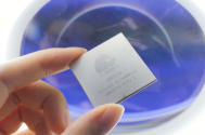
SMIC patent for OPC for EUV.

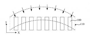
The rule-based optical proximity correction model cannot solve the problem of mask error enhancement factor (MEEF) changes caused by the slit effect. Although the model-based optical proximity correction model can take the slit effect into account, when establishing the model-based optical proximity correction model, different optical proximity correction models must be established at different positions of the slit to construct a holistic Optical proximity correction model. The overall optical proximity correction model consists of multiple sub-models for various slit positions. This causes engineers to have to calibrate each sub-model at different slit positions, which increases the complexity of establishing an optical proximity correction model and easily leads to an increase in modeling error rates.
In order to solve the technical problem, an embodiment of the present invention provides an optical proximity correction method, which is suitable for a photolithography system with an arc-shaped slit, including: providing an original layout graphic; performing outline correction processing on the original layout graphic, so that The outline correction process is suitable for changing the original layout pattern into an arc-shaped pattern consistent with the arc-shaped slit, and the arc-shaped pattern is used as the corrected layout pattern. By changing the original layout pattern into an arc-shaped pattern consistent with the arc-shaped slit, when the photolithography system is used to perform the photolithography process, it is advantageous to make the arc-shaped pattern appear at different positions on the outline of the arc-shaped slit. , the azimuth angle between the incident chief ray of the lithography system and the arc pattern is equal, thereby improving or eliminating the slit effect. Correspondingly, when establishing the optical proximity correction model, the slit effect is reduced or avoided. The impact is that there is no need to establish corresponding optical proximity correction models for different azimuth angles. Therefore, the complexity and error rate of establishing optical proximity correction models are reduced.

It can be seen from the background technology that when technology nodes continue to shrink, an EUV lithography system is usually required. The EUV lithography system has an arc-shaped slit. Moreover, the current EUV lithography system light source is non-telecentric, that is to say, the incident main The light rays and the wafer surface usually have polar angles and azimuth angles. Therefore, the existence of arc-shaped slits will produce a slit effect.

The rule-based optical proximity correction model cannot solve the problem of mask error enhancement factor (MEEF) changes caused by the slit effect. Although the model-based optical proximity correction model can take the slit effect into account, when establishing the model-based optical proximity correction model, different optical proximity correction models must be established at different positions of the slit to construct a holistic Optical proximity correction model. The overall optical proximity correction model consists of multiple sub-models for various slit positions. This causes engineers to have to calibrate each sub-model at different slit positions, which increases the complexity of establishing an optical proximity correction model and easily leads to an increase in modeling error rates.
In order to solve the technical problem, an embodiment of the present invention provides an optical proximity correction method, which is suitable for a photolithography system with an arc-shaped slit, including: providing an original layout graphic; performing outline correction processing on the original layout graphic, so that The outline correction process is suitable for changing the original layout pattern into an arc-shaped pattern consistent with the arc-shaped slit, and the arc-shaped pattern is used as the corrected layout pattern. By changing the original layout pattern into an arc-shaped pattern consistent with the arc-shaped slit, when the photolithography system is used to perform the photolithography process, it is advantageous to make the arc-shaped pattern appear at different positions on the outline of the arc-shaped slit. , the azimuth angle between the incident chief ray of the lithography system and the arc pattern is equal, thereby improving or eliminating the slit effect. Correspondingly, when establishing the optical proximity correction model, the slit effect is reduced or avoided. The impact is that there is no need to establish corresponding optical proximity correction models for different azimuth angles. Therefore, the complexity and error rate of establishing optical proximity correction models are reduced.
Tuojing Technology (Shanghai) semiconductor advanced process equipment R&D and industrialization project capped
According to the news, the semiconductor advanced process equipment R&D and industrialization project is a new R&D and industrialization base built by Tuojing Technology (Shanghai) Co., Ltd., with a planned total investment of 930 million yuan.
The construction area is about 100,000 square meters, which is used to develop advanced ALD thin film process technology and high-capacity equipment platforms, and realize the industrialization of semiconductor equipment required by the customer base centered on Lingang. After the completion of the project, it will better meet the product customization needs of Lingang customers, enhance the company's product formation with Lingang as the center, and form an industrial form covering semiconductor customers and manufacturers in Shanghai and surrounding areas. Guided by market demand, we will carry out independent research and development, break through core technologies, form 100% independent intellectual property products and implement industrialization.

According to the data, Tuojing Technology (Shanghai) Co., Ltd. was established in December 2020 and is a wholly-owned subsidiary of Tuojing Technology Co., Ltd. established in Lingang. Mainly engaged in the research and development, production and sales of high-end integrated circuit thin film equipment. The company focuses on semiconductor thin film deposition equipment and is a domestic dedicated mass-production PECVD, ALD, SACVD, and HDPCVD equipment company.
Jiangsu Xinmeng developed and delivered the first fully automatic precision polishing vertical cleaning machine in China, with a process level of 19nm.
Jiangsu Xinmeng Semiconductor has once again taken an innovative step and announced the successful development and delivery of China's first fully automatic precision polishing vertical cleaning machine.
This equipment combines the advantages of trough Dip and single-chip Spray, and can effectively remove surface particle contaminants after CMP (Chemical Mechanical Polishing), with a process level of astonishing 19 nanometers .
It is reported that the development of a fully automatic precision polishing vertical cleaning machine is another important breakthrough made by Jiangsu Xinmeng in the field of semiconductor manufacturing. This equipment adopts advanced cleaning technology, and through exquisite mechanical design and automated control system, it can effectively remove particle pollutants on the surface after CMP. In addition, this equipment has greatly increased the production capacity of post-CMP cleaning. It is understood that a single fully automatic fine polishing vertical cleaning machine can match the production capacity of 4 CMP machines , which not only greatly improves the overall production efficiency of the CMP process, but also significantly Improved the quality and stability of the CMP process.
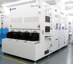
Compared with traditional cleaning methods, the fully automatic precision polishing vertical cleaning machine has higher cleaning accuracy and lower energy consumption. Its unique design makes the cleaning process more uniform and efficient, while reducing manual intervention and reducing uncertainty and errors in the production process. The equipment can realize the following processes:
Immersion loading : Keep the wafer surface in a moist state to avoid cleaning difficulties caused by drying of the grinding fluid on the wafer surface;
Double-sided brushing : remove metal contamination and surface damage on the wafer surface;
SC1 cleaning : Use megasonic waves and SC1 to remove particles and deep defects;
DIW rinse : remove particles that stick to the wafer surface after SC1
Marangoni drying : ensuring the wafer surface is free of contaminants and water marks
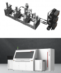
Vacuum welding for IGBT and power semiconductors
KPE-VSS-300 vacuum welding system successfully shipped
The first newly upgraded KPE-VSS-300 vacuum welding system was successfully shipped. The system was independently developed and designed by Kewell Power Semiconductor Division. It has been verified by multiple customer sample trials, and various performance indicators have been Reach the industry-leading level.
In addition to the main system of the vacuum furnace, the KPE-VSS-300 vacuum welding system is equipped with auxiliary equipment such as a vacuum pump box, front and rear connection tables, etc. The main body of the vacuum welding system is divided into 3 chambers, which are preheating, welding and cooling chambers, with good heating and cooling performance; the equipment parameter performance is industry-leading, can reach ultimate vacuum ≤10Pa, long-term working temperature ≤400℃, and uniform temperature The temperature resistance is ≤5℃, the temperature control accuracy is ±1℃, and the void rate is ≤2%.
