Chinese semiconductor thread II

tphuang

Lieutenant General
Staff member
Super Moderator
VIP Professional
Registered Member
Huawei jumping into DUVi because SMEE SSA800 not capable handle Huawei current main stream products in 7nm, 5nm possibly 3nm next year. And Huawei doesn't want to wait for SMEE next improved version.. it may take too long.

Please, Log in or Register to view URLs content!
I would think they are working on EUV project, no DUVi. The timeline doesn't make sense for Huawei DUVi

Some of things we may just have to wait to find out

For thing we are certain is Huawei currently pushing DUVi +SADP scheme hard, such as Mate 70 pro 5nm, and 3nm next year.

The equivalent scanner would be NXT 2050i. Probably this is one Huawei is targeting

Huawei stopped poaching SMEE staffs but it doesn't look like it's giving up DUVi

I believe Huawei is collaborating with SMEE and used SMEE scanner as the foundation for its improved model. After all, they both under central government directive.

Mate 70 pro's chip will be using the latest SMSC process. We really gotta drop this Huawei 7nm stuff

You can't get to the volume that Huawei is at without a whole lot of DUVi and etching tools. There is just no evidence Huawei fab has anywhere close to that much higher end machineries when it has been sanctioned for this long.

Now, I do think there is a good chance Huawei will be on EUV at the same time as SMIC. But that's not for this year
 

jli88

New Member
Registered Member
sir, i have ignore your first massage .. but looks like i need to reply to clarify what NikkeiAsia has done ..

this is two years old news but our beloved Japanese media outlet NikkeiAsia reposted this news with 2024 dates..

first phase R&D has begun in summer 2023 and full fledge research has already started in December 2023 but NikkeiAsia reported Huawei is building new R&D base in Shanghai .. LOL

here is this -
Please, Log in or Register to view URLs content!
this is completely false news because its an old information but they repost this with new date just to mislead innocent people ..
---------------------------------------------------------------------------------------------------------
now let me clarify what is this new R&D base ..

This is Newly build Huawei R&D base just to research new technologies which is revolving around CPU/GPU/Semi equipment/advance semiconductor production methods and build complete ecosystem in mainland. it is not specifically about lithography. though Lithography research also conduct here ..


You are quoting old news, while in 2022, the timeline was 2023 end, recent news even from Shanghai Government puts the timeline for opening this year.

Please, Log in or Register to view URLs content!

Please, Log in or Register to view URLs content!

Please, Log in or Register to view URLs content!

This ofcourse doesn't mean that the research wasn't carried out, limiting my observation to simply the news. Also, the Nikkei Asia China tech and semiconductor news is published by a pretty well informed Taiwanese journalist (who is obviously native in Mandarin).
 

ansy1968

Brigadier
Registered Member
Some of things we may just have to wait to find out

For thing we are certain is Huawei currently pushing DUVi +SADP scheme hard, such as Mate 70 pro 5nm, and 3nm next year.

The equivalent scanner would be NXT 2050i. Probably this is one Huawei is targeting

Huawei stopped poaching SMEE staffs but it doesn't look like it's giving up DUVi

I believe Huawei is collaborating with SMEE and used SMEE scanner as the foundation for its improved model. After all, they both under central government directive.
Sir maybe Huawei may have taken the cudgel in developing the mythical 22nm Duvi synonymous to ASML NXT 2050i.
 

gotodistance

New Member
Registered Member
I would think they are working on EUV project, no DUVi. The timeline doesn't make sense for Huawei DUVi


Mate 70 pro's chip will be using the latest SMSC process. We really gotta drop this Huawei 7nm stuff

You can't get to the volume that Huawei is at without a whole lot of DUVi and etching tools. There is just no evidence Huawei fab has anywhere close to that much higher end machineries when it has been sanctioned for this long.

Now, I do think there is a good chance Huawei will be on EUV at the same time as SMIC. But that's not for this year
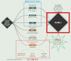
Huawei EUV (SiCarrier and EUV patent sharing and human resources collaboration): ASML ✖

Huawei + SiCarrier

Please, Log in or Register to view URLs content!


Huawei subsidiary SWAYSURE: DRAM Chips (Shenzhen): Samsung, SK-Hynix ✖
Huawei subsidiary PST: Logic Chips (Shenzhen): TSMC, Samsung, Intel ✖
Huawei subsidiary PXW: Image Sensors, RF Chips (Shenzhen): Sony ✖
Huawei Acquisition of SiEn Integrated Circuits: Power Chips (Qingdao): TSMC ✖
Huawei acquisition JHICC: DRAM Chips (Quanzhou, Fujian): Samsung, SK-Hynix ✖
Huawei EUV (SiCarrier and EUV patent sharing and human resources collaboration): ASML ✖
 

gotodistance

New Member
Registered Member
Huawei subsidiary SWAYSURE: DRAM Chips (Shenzhen): Samsung, SK-Hynix ✖
Huawei subsidiary PST: Logic Chips (Shenzhen): TSMC, Samsung, Intel ✖
Huawei subsidiary PXW: Image Sensors, RF Chips (Shenzhen): Sony ✖
Huawei Acquisition of SiEn Integrated Circuits: Power Chips (Qingdao): TSMC ✖
Huawei acquisition JHICC: DRAM Chips (Quanzhou, Fujian): Samsung, SK-Hynix ✖
Huawei EUV (SiCarrier and EUV patent sharing and human resources collaboration): ASML ✖
 

Attachments

  • 2024-03-27_12_24_58.png
    2024-03-27_12_24_58.png
    230.6 KB · Views: 25

tphuang

Lieutenant General
Staff member
Super Moderator
VIP Professional
Registered Member
Huawei subsidiary SWAYSURE: DRAM Chips (Shenzhen): Samsung, SK-Hynix ✖
Huawei subsidiary PST: Logic Chips (Shenzhen): TSMC, Samsung, Intel ✖
Huawei subsidiary PXW: Image Sensors, RF Chips (Shenzhen): Sony ✖
Huawei Acquisition of SiEn Integrated Circuits: Power Chips (Qingdao): TSMC ✖
Huawei acquisition JHICC: DRAM Chips (Quanzhou, Fujian): Samsung, SK-Hynix ✖
Huawei EUV (SiCarrier and EUV patent sharing and human resources collaboration): ASML ✖
right, I think it's reasonable to guess that EUV project is now led by Huawei to some degree.
I don't have any proof of it. There is just a lot of rumors in that direction.
On the recent EUV readiness related comments are from Huawei loyalists
 

tokenanalyst

Brigadier
Registered Member
Mix Silicon-Photonics IC

Butler matrix enabled multi-beam optical phased array for two-dimensional beam-steering and ranging​

Abstract​


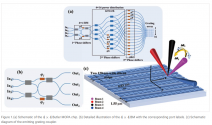
Based on the wavelength transparency of the Butler matrix (BM) beamforming network, we demonstrate a multi-beam optical phased array (MOPA) with an emitting aperture composed of grating couplers at a 1.55 μm pitch for wavelength-assisted two-dimensional beam-steering. The device is capable of simultaneous multi-beam operation in a field of view (FOV) of 60° ×× 8° in the phased-array scanning axis and the wavelength-tuning scanning axis, respectively. The typical beam divergence is about 4° on both axes. Using multiple linearly chirped lasers, multi-beam frequency-modulated continuous wave (FMCW) ranging is realized with an average ranging error of 4 cm. A C-shaped target is imaged for proof-of-concept 2D scanning and ranging.

1714064211376.png

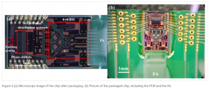
The MOPA chip was fabricated on an 8-inch SOI wafer with a 220-nm-thick silicon layer and a 3-μm-thick buried oxide layer. The chip footprint is 3.5  mm×2.1  mm3.5  mm×2.1  mm. The chip was first wire-bonded to a printed circuit board (PCB). Then, a 45° polished fiber array (FA) was aligned to the four input grating couplers of the chip and fixed by UV-curable adhesive. Figure
Please, Log in or Register to view URLs content!
shows the microscope image of the packaged chip. We used four distributed feedback (DFB) lasers to launch light into the input ports, and a multi-channel voltage source was used to drive the phase shifters of the MOPA chip.

1714064157296.png

Please, Log in or Register to view URLs content!
 

measuredingabens

Junior Member
Registered Member
Please, Log in or Register to view URLs content!

Sweat permeable and ultrahigh strength 3D PVDF piezoelectric nanoyarn fabric strain sensor​

Abstract​

Commercial wearable piezoelectric sensors possess excellent anti-interference stability due to their electronic packaging. However, this packaging renders them barely breathable and compromises human comfort. To address this issue, we develop a PVDF piezoelectric nanoyarns with an ultrahigh strength of 313.3 MPa, weaving them with different yarns to form three-dimensional piezoelectric fabric (3DPF) sensor using the advanced 3D textile technology. The tensile strength (46.0 MPa) of 3DPF exhibits the highest among the reported flexible piezoelectric sensors. The 3DPF features anti-gravity unidirectional liquid transport that allows sweat to move from the inner layer near to the skin to the outer layer in 4 s, resulting in a comfortable and dry environment for the user. It should be noted that sweating does not weaken the piezoelectric properties of 3DPF, but rather enhances. Additionally, the durability and comfortability of 3DPF are similar to those of the commercial cotton T-shirts. This work provides a strategy for developing comfortable flexible wearable electronic devices.
 

tphuang

Lieutenant General
Staff member
Super Moderator
VIP Professional
Registered Member
Please, Log in or Register to view URLs content!

Asensing unveils its MEMS navigation chip which it design, taped out, got produced, tested & packaged. It also developed 6-axis high precision strategic IMU module

Has now received orders from VW, Toyota and Volvo. is getting validated in Europe with 2 luxury German brand. Expect to seal deal in Q3

Also got RFI & RFQ from multiple North American automakers
 
Top