Chinese semiconductor thread II

tokenanalyst

Brigadier
Registered Member

With a total investment of 300 million, another semiconductor project for materials and equipment components in Shanghai has been completed!​


Recently, Shengjian Environment has received great news - the capping ceremony of the Shanghai Shengjian Electronic Special Materials R&D, Manufacturing and Related Resource Resource Project (hereinafter referred to as the "Project") was held grandly!

In January this year, Shengjian Environment held a project groundbreaking ceremony in Xinzhan High-tech Zone, Hefei City. The capping of the factory building this time marks that the project is about to enter a new stage of development. The project is progressing in an orderly and steady manner according to the plan. After the project is put into production, it will facilitate the company's research and development and preparation of related electronic materials, help the company's strategic new business achieve phased results, meet the future production capacity needs of electronic materials, and provide a good foundation for the subsequent electronic materials business. The growth has created a new situation.

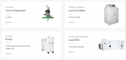
Founded in 2005, Shengjian Environment is a well-known green technology service provider in China's high-tech industry. It was listed on the main board of the Shanghai Stock Exchange in April 2021 (stock code: 603324). The company takes "committed to a better environment" as its corporate mission and continues to adhere to the development policy of "industry extension + product extension". It has formed a main business of "green factory system solutions, semiconductor ancillary equipment and core components, and electronic chemical materials" .
1714055160150.png
Please, Log in or Register to view URLs content!
 

Awenumick

New Member
Registered Member
for now Huawei has ARM license but they are planning to develop its own instruction set..

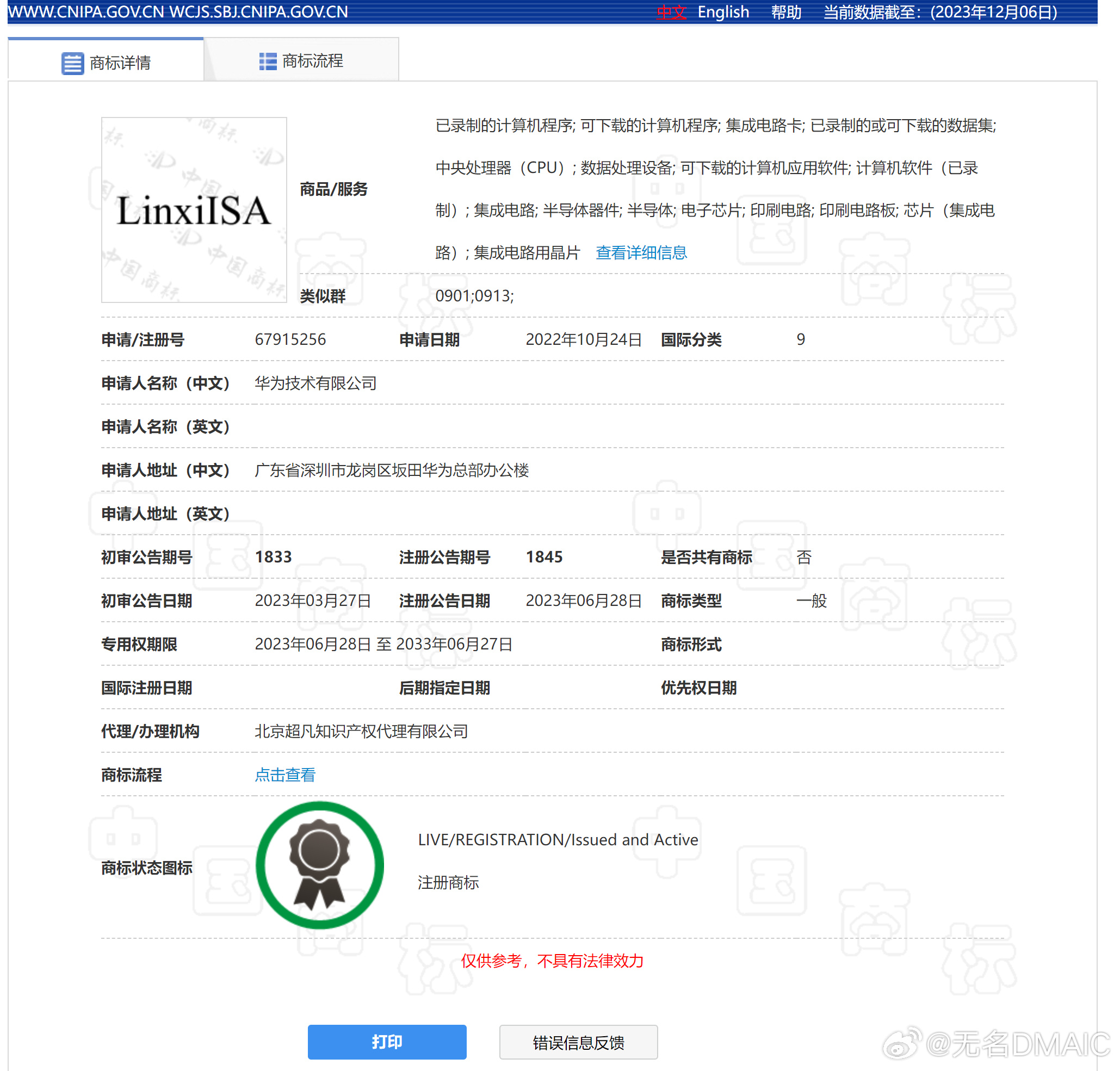
Huawei has registered an instruction set trademark called LinxiISA.. This means Huawei is aiming for complete independence from ARM. Huawei is not just abandoning the ARM architecture but also the ARM instruction set.

Image


Huawei isn't utilizing RISC-V, which is currently the most widely used general instruction set, balancing instruction count and simplification of instruction types.. Huawei has a broader vision

from this year onward, HarmoneyOS completely abandoned the Android base. Mate 70 later this yr will use pure blood Harmony OS HW is looking to have native Harmony OS app for all the apps that Chinese users spend time on.

so in near future i can see Loongson might use Huawei's architecture design if ARM revoke license.
I believe LinxiISA is their nuclear option, in case they get blocked from accessing ARM. It would've been nice had they joined forces with alibaba and used risc-v instead though. That way they wouldn't get completely cut off from the wider risc-v ecosystem. Just my opinion.
 

Oldschool

Junior Member
Registered Member
SMIC is currently building 340,000 wpm of 28nm capacity. They could use the 28nm machine if it existed.
Other companies like Nexchip will also be building some 28nm capacity. It is required for high-end DDICs, automotive MCUs, IoT, etc.


They could stop Chinese companies from using US IP and patents. Unfortunately SiFive recently submitted a patent for instruction fusion on RISC-V.
Please, Log in or Register to view URLs content!

So that could be an issue. It will be hard to implement high-end RISC-V processors without this.
The best way to counter this will be for Chinese RISC-V companies to develop their own patents.
Huawei jumping into DUVi because SMEE SSA800 not capable handle Huawei current main stream products in 7nm, 5nm possibly 3nm next year. And Huawei doesn't want to wait for SMEE next improved version.. it may take too long.

Please, Log in or Register to view URLs content!
 

daifo

Captain
Registered Member
If China was desperate enough, they would ignore Intel patents. I expect the new cold war to get so intense in the future that all patents will be ignored. I expect US to first ignore Chinese patents citing "national security" and then China will follow suit.

The fundamental patents are expiring as time goes by...that is probably why they are not chasing after Zhaoxin (whom may also own intellectual property via VIA/Cyrix). However they can always introduce new ones and make them very important to modern software execution.
 

sunnymaxi

Captain
Registered Member
Huawei jumping into DUVi because SMEE SSA800 not capable handle Huawei current main stream products in 7nm, 5nm possibly 3nm next year. And Huawei doesn't want to wait for SMEE next improved version.. it may take too long.

Please, Log in or Register to view URLs content!
sir, i have ignore your first massage .. but looks like i need to reply to clarify what NikkeiAsia has done ..

this is two years old news but our beloved Japanese media outlet NikkeiAsia reposted this news with 2024 dates..
GK5mIyIa8AAcIoe.png

first phase R&D has begun in summer 2023 and full fledge research has already started in December 2023 but NikkeiAsia reported Huawei is building new R&D base in Shanghai .. LOL

here is this -
Please, Log in or Register to view URLs content!

this is completely false news because its an old information but they repost this with new date just to mislead innocent people ..
---------------------------------------------------------------------------------------------------------
now let me clarify what is this new R&D base ..

This is Newly build Huawei R&D base just to research new technologies which is revolving around CPU/GPU/Semi equipment/advance semiconductor production methods and build complete ecosystem in mainland. it is not specifically about lithography. though Lithography research also conduct here ..

----------------------------------------------------------------------------------------------------------
Huawei deeply involved in EUV project not in DUVi .. Huawei tried to buy SMEE whole , also pouched talent from SMEE but local authorities intervened so they discarded the idea.

Huawei is just one player in whole team of Lithography just to help other institutes to establish domestic supply chain. they just cannot build entire machine themselves ..

CIOMP is almost finished first LPP EUV prototype..

we have first clear cut evidence of Huawei's involvement in EUV project.

last week, PengCheng Lab EUV light source control patent has been authorized. PengCheng Lab is owned by Huawei ..
PengCheng Lab EUV light source control patent has been authorized.png

another information to be clear..

SMEE's SSA800i is already upgraded to ASML's 2000i .. in last Quarter 2023, they just officially published the overlay Metrology tool and specifically mentioned 7nm ..

from this year, SMEE will start volume production of lithography include dry+immersion .. this is also a confirmed news..

i fully agreed with you here. SMEE pace is not good. they are slow but if look at the history of SMEE, they started very late. actually work begun after 2020.. but if i tell the history of SMEE before 2020 time period. people will be shocked how lazy and careless they were at that time .. at that time, SMEE consists of some old dudes just to use foreign made components/parts..

now situation is completely reverse. they have grown into a giant company.. total employees cross 2500 mark. total R&D force are now in hundreds. all are PHDs ..
 
Last edited:

Oldschool

Junior Member
Registered Member
sir, i have ignore your first massage .. but looks like i need to reply to clarify what NikkeiAsia has done ..

this is two years old news but our beloved Japanese media outlet NikkeiAsia reposted this news with 2024 dates..
View attachment 128602

first phase R&D has begun in summer 2023 and full fledge research has already started in December 2023 but NikkeiAsia reported Huawei is building new R&D base in Shanghai .. LOL

here is this -
Please, Log in or Register to view URLs content!

this is completely false news because its an old information but they repost this with new date just to mislead innocent people ..
---------------------------------------------------------------------------------------------------------
now let me clarify what is this new R&D base ..

This is Newly build Huawei R&D base just to research new technologies which is revolving around CPU/GPU/Semi equipment/advance semiconductor production methods and build complete ecosystem in mainland. it is not specifically about lithography. though Lithography research also conduct here ..

----------------------------------------------------------------------------------------------------------
Huawei deeply involved in EUV project not in DUVi .. Huawei tried to buy SMEE whole , also pouched talent from SMEE but local authorities intervened so they discarded the idea.

Huawei is just one player in whole team of Lithography just to help other institutes to establish domestic supply chain. they just cannot build entire machine themselves ..

CIOMP is almost finished first LPP EUV prototype..

we have first clear cut evidence of Huawei's involvement in EUV project.

last week, PengCheng Lab EUV light source control patent has been authorized. PengCheng Lab is owned by Huawei ..
View attachment 128604

another information to be clear..

SMEE's SSA800i is already upgraded to ASML's 2000i .. in last Quarter 2023, they just officially published the overlay Metrology tool and specifically mentioned 7nm ..

from this year, SMEE will start volume production of lithography include dry+immersion .. this is also a confirmed news..

i fully agreed with you here. SMEE pace is not good. they are slow but if look at the history of SMEE, they started very late. actually work begun after 2020.. but if i tell the history of SMEE before 2020 time period. people will be shocked how lazy and careless they were at that time .. at that time, SMEE consists of some old dudes just to use foreign made components/parts..

now situation is completely reverse. they have grown into a giant company.. total employees cross 2500 mark. total R&D force are now in hundreds. all are PHDs ..
Some of things we may just have to wait to find out

For thing we are certain is Huawei currently pushing DUVi +SADP scheme hard, such as Mate 70 pro 5nm, and 3nm next year.

The equivalent scanner would be NXT 2050i. Probably this is one Huawei is targeting

Huawei stopped poaching SMEE staffs but it doesn't look like it's giving up DUVi

I believe Huawei is collaborating with SMEE and used SMEE scanner as the foundation for its improved model. After all, they both under central government directive.
 
Last edited:

tokenanalyst

Brigadier
Registered Member

Expand cooperation and work together for win-win results! Maiwei Co., Ltd. delivers OLED bending laser cutting equipment to Tianma.​


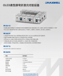
Maiwei Technology successfully delivered its second OLED flexible screen bending laser cutting (Bending Cut) equipment to its long-term partner, Xiamen Tianma Display Technology Co., Ltd. (hereinafter referred to as "Tianma Display Technology"), which will be used in its 6th generation Flexible AMOLED production line - mass production of mobile phone screens, smart wearable screens and car screens.This is another key project of cooperation between the two parties after the company delivered 5 OLED laser cutting equipment at the beginning of this year .

1714059062067.png

This equipment of Maiwei Co., Ltd. is mainly used for the cutting, peeling and curing process of the support film in the bending area of the OLED flexible panel screen. It mainly includes automatic loading and unloading, cutting, peeling, curing, testing and other units, with an efficient and economical process. The bending radius is reduced and better bending effect is achieved. Maiwei Co., Ltd. is the only company in China that has successfully developed and mass-produced this equipment.

At the end of 2021 , the company's first-generation OLED bending laser cutting equipment independently developed and the first domestic OLED bending laser cutting equipment won the bid for BOE's 6th -generation AMOLED production line project. After more than two years of mass production verification, it has achieved a significant improvement in product yield for the client. Improvement, as well as reduction of labor costs, material costs and material losses.

Through continuous process optimization and equipment upgrading, Tianma Display Technology’s second-generation bending laser cutting equipment was delivered this time. Compared with the previous generation equipment, the operation mode has been optimized, with higher efficiency, higher utilization rate, stronger maintainability, and better production The beat is more in line with customer needs.​

Please, Log in or Register to view URLs content!
 

tokenanalyst

Brigadier
Registered Member

With a total investment of 300 million, another semiconductor project for materials and equipment components in Shanghai has been completed!​


Recently, Shengjian Environment has received great news - the capping ceremony of the Shanghai Shengjian Electronic Special Materials R&D, Manufacturing and Related Resource Resource Project (hereinafter referred to as the "Project") was held grandly!

In January this year, Shengjian Environment held a project groundbreaking ceremony in Xinzhan High-tech Zone, Hefei City. The capping of the factory building this time marks that the project is about to enter a new stage of development. The project is progressing in an orderly and steady manner according to the plan. After the project is put into production, it will facilitate the company's research and development and preparation of related electronic materials, help the company's strategic new business achieve phased results, meet the future production capacity needs of electronic materials, and provide a good foundation for the subsequent electronic materials business. The growth has created a new situation.

Founded in 2005, Shengjian Environment is a well-known green technology service provider in China's high-tech industry. It was listed on the main board of the Shanghai Stock Exchange in April 2021 (stock code: 603324). The company takes "committed to a better environment" as its corporate mission and continues to adhere to the development policy of "industry extension + product extension". It has formed a main business of "green factory system solutions, semiconductor ancillary equipment and core components, and electronic chemical materials" .
View attachment 128601
Please, Log in or Register to view URLs content!
 

olalavn

Senior Member
Registered Member
Huawei nhảy vào DUVi vì SMEE SSA800 không đủ khả năng xử lý các sản phẩm dòng chính hiện tại của Huawei ở tiến trình 7nm, 5nm có thể là 3nm vào năm tới. Và Huawei không muốn đợi SMEE phiên bản cải tiến tiếp theo.. có thể sẽ mất quá nhiều thời gian.

Please, Log in or Register to view URLs content!
because SMEE and ASML signed cross patents... that's why SMEE couldn't launch sooner than expected... Huawei jumped in since 2020... that project is finished, there are many rumors about the 9010 chip used their lithography
 

tphuang

Lieutenant General
Staff member
Super Moderator
VIP Professional
Registered Member

With a total investment of approximately 2.8 billion yuan, Xinhua Semiconductor’s annual 10,000-ton electronic-grade polysilicon project was completed.​


On April 18, Mengyuan Sixth Construction announced that Inner Mongolia Xinhua Semiconductor Technology Co., Ltd.’s 10,000 tons per year high-purity electronic grade polysilicon industrial cluster project was successfully completed. The project is located in Zhonghuan Industrial Park, Jinhe Town, Saihan District, Hohhot City, Inner Mongolia. The project covers an area of 216,450 square meters, with a total construction area of 153,000 square meters, and a total investment of approximately 2.8 billion yuan.

It is reported that after the project is completed and reaches production, it can achieve long-term and stable supply to global customers with an annual production capacity of 10,000 tons of high-purity electronic grade polysilicon, 500 tons of electronic grade dichlorodihydrogen silicon, 3,000 tons of electronic grade trichlorosilane and electronic grade tetrahydrogen silicon. Silicon chloride has a production capacity of 3,000 tons to meet the global semiconductor market demand.

The project started on September 1, 2022. The Inner Mongolia Branch's construction scope includes: post-processing (including three-dimensional storage, desalted water, high-purity water, silicon core drawing, laboratories, etc.), reduction (water-containing system and corridor), precision Distillation (including intermediate tank area), exhaust gas recovery, electronic special gas, zone melting workshop, construction and installation engineering of all devices, and pipes, cables and instrument cables between each device are based on the feeding system. Currently, it has entered the trial production stage.

Please, Log in or Register to view URLs content!
Does anyone know what kind of market share China has on semi grade polysilicon? This seems like something China should dominate considering how much they control the solar grade polysilicon
 
Top