You are using an out of date browser. It may not display this or other websites correctly.
You should upgrade or use an alternative browser.
You should upgrade or use an alternative browser.
Chinese semiconductor thread II
- Thread starter vincent
- Start date
Still waiting until SMEE finally announces and then after that it is proven that it has built a DUVi machine equivalent at least to the mid range level of performance of those of ASML, Canon, and Nikon, using entirely domestically made equipment. When this happens, China will at least be free, because doing so will mean that China will also have solved its lapses in aligning and other necessary metrological equipment in chip making.SMEE's DUV is all tied up in patents, and there has been almost no news about it since 2022, but patents are still being released by lithography research companies about the DUV-DUV-I -EUV is still released every month...
When it finally happens it will be a massive moment in history for China. But I feel when it happens you won't feel the hype because few will cover it.Still waiting until SMEE finally announces and then after that it is proven that it has built a DUVi machine equivalent at least to the mid range level of performance of those of ASML, Canon, and Nikon, using entirely domestically made equipment. When this happens, China will at least be free, because doing so will mean that China will also have solved its lapses in aligning and other necessary metrological equipment in chip making.
When the ws15 engines were ready for j20, for some reason there was not much impact as expected. Maybe it's China's strategy to keep everything under wraps even big breakthroughs. That way by the time you know China has it, it's too late. Better being like India and announcing every single thing for the world to hear.
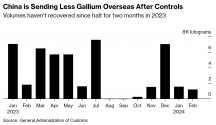
China shipped out about 2,760 kilograms of gallium in the first two months of 2024, down from 8,865 kilograms a year earlier. The biggest buyers were Japan at 1,000 kilograms, South Korea at 900 kilograms and Germany at 500 kilograms.
China is still exporting too much Ga. Even if we ignore the military applications of Ga, you are hurting your own domestic producers of GaN & GaA when you allow exports
VeriSilicon Hainan R&D Center newly renovated and opened
VeriSilicon Microelectronics (Hainan) Co., Ltd. (hereinafter referred to as "VeriSilicon Hainan") held the opening ceremony of the VeriSilicon Hainan R&D Center in the brand-new Haikou office . Liu Liwu, Secretary of the Party Leadership Group and Director of the Hainan Provincial Department of Industry and Information Technology, Ma Yonghua, Secretary of the Party Committee and Director of the Hainan Provincial State-owned Assets Supervision and Administration Commission, Feng Yong, Vice Mayor of Haikou Municipal People’s Government, Zhu Jun, Secretary of the Meilan District Committee of Haikou City, Haikou National High-tech Kang Zhongxian, deputy director of the Industrial Development Zone Management Committee, Dr. Dai Weimin, VeriSilicon founder, chairman and president, VeriSilicon's senior management team, partner representatives and employee representatives from all regions attended the ceremony to witness the opening of the new VeriSilicon Hainan R&D Center.
In December 2020, VeriSilicon Hainan was registered and established in Haikou National High-tech Industrial Development Zone. Relying on VeriSilicon's deep semiconductor IP reserves and mature technical experience and application solutions, combined with Hainan's industrial foundation and planning layout, the company focuses on the smart medical and rehabilitation industry. VeriSilicon Hainan has been committed to promoting Hainan’s talent localization strategy. Up to now, VeriSilicon’s Hainan R&D personnel account for as high as 90%, of which 40% are from Hainan and 80% graduated from Hainan University.
In December 2020, VeriSilicon Hainan was registered and established in Haikou National High-tech Industrial Development Zone. Relying on VeriSilicon's deep semiconductor IP reserves and mature technical experience and application solutions, combined with Hainan's industrial foundation and planning layout, the company focuses on the smart medical and rehabilitation industry. VeriSilicon Hainan has been committed to promoting Hainan’s talent localization strategy. Up to now, VeriSilicon’s Hainan R&D personnel account for as high as 90%, of which 40% are from Hainan and 80% graduated from Hainan University.
Xioduan Chengdu R&D Center project signing, involving CPU
According to information released by Chengdu and the Development and Reform Bureau of Chengdu High-tech Zone, the signing ceremony of the industrial transfer cooperation project was held at the opening ceremony of the 2024 China Industrial Transfer Development Docking Event (Sichuan). Chengdu High-tech Zone and Xiaoduan (Shenzhen) Computing Technology Co., Ltd. signed an on-site contract on the Xiaoduan Chengdu R&D Center project, the only project promoted in Chengdu at this event.
According to reports, the total investment in the project is 2 billion yuan to carry out the design and research and development of large computing power CPU chips suitable for AI servers. It meets the requirements for CPU high performance, low power consumption, and high security, and can be widely used in AI/HPC large computing power clusters, government, finance, e-commerce, and digital cultural and creative fields.
The project products will use innovative accelerators and interconnection technologies based on the ARM instruction set to significantly improve performance for application scenarios such as edge, cloud, and large computing power networking; they will have the advantages of flexible combination, high performance, and high cost performance. On the one hand, it can provide cloud users with more virtual machines and increase the density of application deployment on a single server; on the other hand, it can effectively improve the resource management and communication efficiency of ultra-large-scale computing clusters.
Information shows that Xioduan (Shenzhen) Computing Technology Co., Ltd. is a cutting-edge company focusing on R&D and technological innovation in the field of cloud computing, mainly focusing on the design and development of ARMServer architecture CPU chips and solutions.
Dongfang Jingyuan appears at SEMICON China 2024, leading the development and reform of yield management with innovation
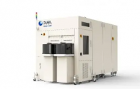
At this exhibition, Dongfang Jingyuan brought a new generation of electron beam measurement and inspection equipment, including defect re-inspection equipment DR-SEM, measurement equipment CD-SEM, defect inspection equipment EBI, and a product that integrates yield data, defects YieldBook is a yield management system that integrates data and measurement data collection and analysis.
Dongfangjingyuan DR-SEM has entered the head client verification, and the verification results of technical indicators such as image quality, algorithm (D2D) and CR (>95%) meet the mass production requirements. It is worth mentioning that the self-developed optical window OM imaging system not only reduces foreign supply chain risks, but also has been unanimously recognized by customers for its verification of the Auto Bare wafer review function, which can meet the re-inspection requirements for 70nm defects. At the same time, combined with the upcoming new generation of self-developed EOS and DUV inspection systems, it is expected to meet the needs of advanced manufacturing processes for unpattern wafer defect re-inspection.

The new generation 12-inch CD-SEM model SEpA-c430 has achieved comprehensive improvements in measurement performance and speed. The measurement repeatability reaches 0.25nm, meeting the needs of 28nm production lines. At the same time, through improved electron beam scanning and signal detection, production capacity has been increased by 30%. The newly launched wafer surface charge compensation function can improve ADI layer measurement capabilities. In addition, the SEpA-c310 launched for the third-generation semiconductor market not only achieves 6/8-inch compatibility, but also achieves compatibility with different materials and thicknesses (such as GaN/SIC), which has been implemented by multiple head customers. It has passed mass production verification and entered the mass production line.

Dongfang Jingyuan’s 12-inch EBI continues to iterate and improve detection capabilities. The new generation SEpA-i525 model adopts continuous scanning mode, enriches the Negative mode detection method, increases the maximum beam current to 40nA, adds functions such as Flooding Gun, and has a higher production capacity than the previous generation. The model has been increased by more than 3 times, the application field has been expanded from logic Fab to memory Fab, and the new product has entered the Fab verification of many domestic leading customers.
Computational lithography platform PanGen adds new products

PanGen Yield Comprehensive Optimization System is a computational lithography software product of Dongfang Jingyuan. This product has OPC optimization functions suitable for mature process nodes. It is also the first full-chip inverse lithography (ILT) with a CPU+GPU hybrid architecture. ) function of the mask optimization tool. Reverse lithography has proven to be an effective mask optimization technique for projecting lithography-limited process nodes.
Xinhe Semiconductor won the Annual Technology Breakthrough EDA Company Award at the 2024 China IC Design Achievement Award
The project applied by Xinhe Semiconductor this time is a one-stop multi-physics simulation EDA solution for the chiplet field , including Chiplet advanced packaging electromagnetic simulation platform Metis, Chiplet integrated chip multi-physics simulation platform Notus, Chiplet high-speed interconnect signal integrity The simulation platform Channel Expert covers signal integrity, power integrity, electromagnetic interference, thermal and stress reliability, etc. It successfully helps designers quickly and accurately solve multi-physics problems under the Chiplet architecture, effectively accelerating products based on the Chiplet architecture. Development and optimization iterations.
At present, chiplet technology based on 2.5D\3D advanced packaging has become a key strategic direction for the semiconductor industry to break through the computing power bottleneck. Especially in the field of high-performance computing chips, the application scenarios of this technology are particularly broad. It is suitable for artificial intelligence training and automatic assisted driving. Diversified market demands such as upgrades and improvements in smart terminal experience have played a crucial role.
This breakthrough EDA technology independently developed by Xinhe Semiconductor has fully integrated with the world's mainstream Chiplet manufacturing process by virtue of its excellent cross-scale simulation capabilities, AI-driven adaptive meshing technology and distributed parallel computing capabilities loaded by cloud computing. , seamlessly integrated into the global Chiplet ecosystem, and successfully used in the development of the latest generation of high-performance computing chip products by many leading international companies.
I doubt there will ever be an announcement.until SMEE finally announces

