Chinese semiconductor thread II

tokenanalyst

Brigadier
Registered Member

SMIC's "Semiconductor Device and Formation Method" Patent Authorized​

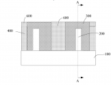
SMIC International Integrated Circuit Manufacturing (Beijing) Co., Ltd. recently obtained a patent called "Semiconductor Device and Formation Method". The authorization announcement number is CN111900088B. The authorization announcement date is March 26, 2024. The application The date is May 5, 2019.
1712068741656.png


The present invention provides a semiconductor device and a method for forming the same, which includes the steps of: providing a substrate with a plurality of spaced and arranged fins formed on the substrate; forming a dummy gate structure across the fins on the substrate; A first interlayer dielectric layer is formed on the substrate and on the sidewall of the dummy gate structure, and the top of the first interlayer dielectric layer is lower than the top of the dummy gate structure; defining cut-off opening pattern; etching the dummy gate structure along the cutting opening pattern until the substrate is exposed to form a cutting opening; forming a second interlayer dielectric layer on the first interlayer dielectric layer, And the second interlayer dielectric layer fills the cutting opening, and the top of the second interlayer dielectric layer is flush with the top of the dummy gate structure; the present invention makes the performance of the formed semiconductor device stable.​


Please, Log in or Register to view URLs content!
 

dropout003

New Member
Registered Member
Exactly, its said the ion implantation is next to lithography in terms of difficulty, back in the day most of China ion implantation industry was focus on solar (Kingstone and mostly CETC), now there are 3 localized companies competing in the integrated circuit ion implantation space in just few years, increasing their products offering from a few products to a whole production lines, now the cover high end IC process, third generation semiconductors and solar.
I have been saying this for years people underestimate how fast things can change with disruptive market changes like US export controls. Like nature, companies are going to try to fill void niches as soon as possible.​
Why is domestic share of ion implanters still low (at least when compared to deposition and etching)?
 
  • Like
Reactions: jwt

tokenanalyst

Brigadier
Registered Member

Jiufengshan Laboratory + Huazhong University of Science and Technology jointly tackled key problems, and a new photoresist technology completed preliminary process verification.​


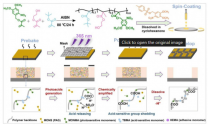
Recently, Jiufengshan Laboratory and Huazhong University of Science and Technology formed a joint research team to rely on the Jiufengshan Laboratory process platform to support the Huazhong University of Science and Technology team to break through the "double non-ionic photoacid synergistically enhanced response chemical amplification photoresist" technology.​

1712069053572.png

Recently, Jiufengshan Laboratory and Huazhong University of Science and Technology formed a joint research team to rely on the Jiufengshan Laboratory process platform to support the Huazhong University of Science and Technology team to break through the "chemical amplification photoresist with dual non-ionic photoacid synergistically enhanced response" technology. This photoresist system with independent intellectual property rights has completed preliminary process verification on the production line, and simultaneously completed the detection and optimization of various technical indicators, realizing the entire chain from technology development to achievement transformation.

1712069000917.png

Through ingenious chemical structure design, this research uses two photosensitive units to construct a "chemical amplification photoresist with dual non-ionic photoacid synergistically enhanced response", and finally obtains photolithographic image morphology, excellent line edge roughness, and space pattern width. The standard deviation (SD) of the value normal distribution is extremely small (about 0.05), the performance is better than most commercial photoresists, and the time required for each photolithography and development step fully meets the requirements for throughput and production efficiency in semiconductor mass production manufacturing. need.

The research results are expected to provide clear directions for common problems in photolithography manufacturing, and at the same time provide technical reserves for the development of EUV photoresists.

Please, Log in or Register to view URLs content!
 

tokenanalyst

Brigadier
Registered Member

Compound semiconductor project in Wuhan completed​


On April 1, according to the Nanguanggu public account, the completion ceremony of the high-power blue semiconductor laser industrialization project built by Wuhan Xinweiyuan Electronic Technology Co., Ltd. (hereinafter referred to as "Wuhan Xinweiyuan") with a total investment of 1 billion yuan was held at the bridge. Intelligent Manufacturing Industrial Park was held.

According to reports, the project has a plant area of more than 10,000 square meters and is mainly building a high-power blue-light semiconductor laser production line based on semiconductor compound (GaN) technology. At present, the factory building and supporting decoration have been completed, and various equipment and instruments are being debugged. It is planned to be officially put into production in January 2025.

Public information shows that Wuhan Xinweiyuan is engaged in the design and development of high-power blue-light semiconductor laser-related materials, chips, packaging, etc., as well as product R&D, manufacturing and sales, and is committed to realizing the industrialization of domestic high-power blue-light semiconductor lasers.

According to Wuhan’s official website, at present, the company’s products mainly include high-power blue light LD, laser display light source components and laser headlight source components.​

Please, Log in or Register to view URLs content!
 

tphuang

Lieutenant General
Staff member
Super Moderator
VIP Professional
Registered Member
Please, Log in or Register to view URLs content!
we got 峰岹科技 here using RISC-V to develop MCUs for robotic ECU. Says they are focused on just using 40nm process

Please, Log in or Register to view URLs content!
another company here 正达半导体 with 1 million SiC substrate production project

Please, Log in or Register to view URLs content!
first domestic auto imaged infrared camera production has gone online in Gaode's subsidiary 轩辕智驾 (xy-idrive)
to be used by Deepway truck, Shacman trucks, GAC Aion & Dongfeng Mengshi

Please, Log in or Register to view URLs content!
Sia Micro on its MEMS business in Beijing (Fab 3). Says they are maintaining gross margin of 35.99% this past year. They've expanded into new products in MEMS-OCS, BAW filter, MEME mirror
 

tokenanalyst

Brigadier
Registered Member
FE-SEM company is getting financing for the R&D of SEM application in semiconductors.​

Huiran Technology’s semiconductor measurement equipment headquarters project was signed and landed in Wuxi with a total investment of 1 billion yuan​


On April 1, the Huiran Technology Semiconductor Measurement Equipment Headquarters project with a total investment of 1 billion yuan was officially signed and landed in Binhu District, Wuxi City. It is reported that Huiran Technology Co., Ltd. is a high-tech enterprise with electron optical technology as its core and focusing on the research and development, production and sales of scanning electron microscopes and semiconductor measurement equipment. The projects signed and implemented this time include the company's headquarters, listed entities and newly established semiconductor measurement equipment R&D and production bases.

Please, Log in or Register to view URLs content!
 

tokenanalyst

Brigadier
Registered Member

Ultra-Fast Source Mask Optimization via Conditional Discrete Diffusion​


Abstract:
Source mask optimization (SMO) is vital for mitigating lithography imaging distortions caused by shrinking critical dimensions in integrated circuit fabrication. However, the computational intensity of SMO, involving multiple integrals in Abbe’s theory, hinders its widespread adoption and advancement. In this paper, we present Diff-SMO, a highly efficient and accurate SMO framework with a primary emphasis on enhancing source optimization techniques. Previous research was confined to mask optimization acceleration due to the constraints of the academia lithography model. Diff-SMO extends the scope of optimization by concurrently refining the intricate interplay between the source and mask. We first develop a GPU-accelerated lithography simulator grounded in Abbe’s theory, enabling full GPU acceleration throughout the SMO process. Furthermore, we propose a discrete diffusion model for generating quasi-optimal sources, significantly improving computational efficiency. Our experimental results demonstrate exceptional imaging fidelity, surpassing the state-of-the-art, with over 200 times higher throughput compared to traditional SMO methods.​

Please, Log in or Register to view URLs content!
 

tokenanalyst

Brigadier
Registered Member
More advancement in MultiBeam lithography. Important for mask production.

Huazhong University of Science and Technology has made new progress in the direction of micro-nano manufacturing based on precise control of electron beams​


Recently, "Nature Communications" published online the "Huazhong University of Science and Technology-Huayinxin (Wuhan) Technology Co., Ltd. New Semiconductor Display Light Source Joint Research Center" titled "Boosting the electron beam transmittance of field emission cathode using a self-charging gate" research results.

Electron beam focusing technology can be achieved by applying an external electric field or magnetic field, and has the characteristics of high resolution, precise control, non-contact processing and wide application range. This technology is widely used in chip manufacturing in the semiconductor industry, nanostructure preparation in the field of nanofabrication, mask production in the photolithography field, and display imaging in the light source field.

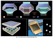
As shown in the figure, the research team deposited a layer of electret material silicon nitride (SiN x ) on the surface of the device. The Si³⁺ trap center inside the SiN x electret can capture and stably store electrons. When electrons are emitted to the surface of the device, the device captures the electrons for charging. The charged device surface is negatively charged, thereby achieving a stable focusing effect on subsequent electrons. Different from traditional electron beam focusing schemes, this new electron beam focusing scheme does not require the introduction of additional electrostatic fields or magnetic fields, providing new possibilities for precise control of electron beams and having important application prospects in the field of micro-nano manufacturing.

1712075557236.png

Please, Log in or Register to view URLs content!
 

mst

Junior Member
Registered Member
Please, Log in or Register to view URLs content!


US asks South Korea to toughen up export controls on China chips
US officials discussed the issues in depth with the government of South Korean President Yoon Suk Yeol in March. While the US is trying to reach an agreement before a G7 summit in mid-June, Seoul officials are debating whether to satisfy the US request, in part because China remains a key trading partner.
 
Top