Chinese semiconductor thread II

tokenanalyst

Lieutenant General
Registered Member
Really interesting, this could push logic devices to operate under extreme current condictions.​

The Suzhou Institute of Nano-Tech and Nano-Bionics, Chinese Academy of Sciences, has made a series of advances in gallium oxide vertical power devices through its nanofabrication platform.​


Gallium oxide (Ga2O3), an ultrawide bandgap semiconductor, possesses advantages such as high critical breakdown field strength, high saturated electron drift velocity, intrinsic solar-blind ultraviolet response, and low-cost fabrication on large-size single-crystal substrates using fusible methods. In recent years, it has attracted widespread attention in power radio frequency electronics, deep ultraviolet detection, piezoelectricity, ferroelectricity, and intelligent sensing. The National 15th Five-Year Plan outlines the promotion of the industrialization of ultrawide bandgap semiconductors such as gallium oxide and diamond, further highlighting their strategic value. Vertical power devices, which utilize a vertical drift layer to handle high voltage while simultaneously increasing the current carrying capacity per unit chip area, are core devices for leveraging the performance advantages of gallium oxide.

Recently, the Suzhou Institute of Nano-Tech and Nano-Bionics (SINANO) Nanofabrication Platform, in collaboration with the University of Science and Technology of China (USTC), Nanjing University, Henan Normal University, and the University of Electronic Science and Technology of China (UESTC), has made a series of advancements in gallium oxide vertical power devices. The research focuses on vertical fin field-effect transistors (FinFETs), current aperture vertical electron transistors (CAVETs), trench gate metal-oxide-semiconductor field-effect transistors (UMOSFETs), and Schottky barrier diodes (SBDs). Techniques developed include localized bottom dielectric electric field modulation, all-ion implantation planar processes, MOCVD sidewall re-epitaxy, HF sidewall wet processing, buried field shielding, and composite edge termination. The relevant results will be published at the 38th IEEE International Symposium on Power Semiconductor Devices and Integrated Circuits in 2026.nal Symposium on Power SemicoInductor Devices and ICs, ISPSD), Applied Physics Letters, etc.
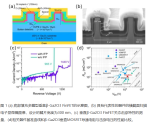
1784046809239.png

Please, Log in or Register to view URLs content!
 

tokenanalyst

Lieutenant General
Registered Member

The headquarters project of Nanotron Semiconductor was signed and settled in Wuzhong District, Suzhou.​

The signing ceremony for the Nanotron Semiconductor headquarters project took place in Wuzhong District, Suzhou, attended by key officials including Liu Jinbao, General Manager of Suzhou Natron Zhiyuan Semiconductor Technology Co., Ltd., and Wan Li, Secretary of the Wuzhong District Committee. Founded in 2025, the company specializes in precision dispensing and fluid control for advanced semiconductor packaging, with self-developed equipment that has achieved industry-leading precision and secured orders from major players in the field. The new headquarters will be established in the Chip Valley Science and Technology Innovation Park within Wuzhong High-tech Zone, aiming to enhance the local semiconductor industry layout by leveraging independent core technologies to strengthen supply chains and support the growth of the third-generation semiconductor sector.

Wuzhong District has strategically prioritized third-generation semiconductors, utilizing the Core Valley Science and Technology Innovation Park to foster industrial incubation, R&D, and commercialization. This initiative has attracted high-quality firms in advanced materials, packaging equipment, and power devices, creating a synergistic industrial ecosystem. The arrival of Nanotron Semiconductor addresses critical gaps in advanced packaging and precision fluid dynamics equipment, accelerating the formation of a specialized innovation cluster. Moving forward, Wuzhong District commits to providing comprehensive enterprise support to ensure rapid project implementation, while the company plans to increase R&D investment to drive localization and innovation in advanced packaging equipment, collectively boosting the regional semiconductor industry's competitiveness.​

Please, Log in or Register to view URLs content!
 

tokenanalyst

Lieutenant General
Registered Member

The Guojing Semiconductor Thousand-ton-level Large-Size Silicon Single Crystal Project, with a total investment of 1 billion yuan, has​

Recently, the groundbreaking ceremony for Guojing Semiconductor's 1,000-ton-per-year large-size silicon single crystal project was held in Baotou Rare Earth High-tech Zone.

It is reported that the project has a total investment of 1 billion yuan, covers an area of approximately 177 mu, and plans to build a 50,000-square-meter standardized monocrystalline production plant, equipped with 140 sets of monocrystalline furnace production equipment. The entire project is scheduled to be completed and put into operation in December 2027.

Once the project reaches full production capacity, it will have an annual production capacity of over 1,000 tons of integrated circuit-grade monocrystalline silicon, with products covering core categories such as integrated circuit substrate silicon wafers and special silicon components for semiconductor etching equipment, widely supplying strategic fields such as chip manufacturing and high-end semiconductor equipment.


Guojing Semiconductor Materials (Baotou) Co., Ltd. is a wholly-owned subsidiary of GRINM Semiconductor Silicon Materials Co., Ltd., and is fully responsible for the construction and operation of this project.​

Please, Log in or Register to view URLs content!
 

tokenanalyst

Lieutenant General
Registered Member
Which ceremony was this for ?
I guess that ASML knew that SMEE was going in their way to develop their next generation of FrontEnd lithography machines (ArFi, ArF, KrF and I-Line), they feared that the government was going to enforce the use of SMEE machines, they are the ones pouring the money for these chips projects, so instead of threatening a patent and trade war with China they told to SMEE bosses at the time "stay in your lane (packaging) and we going to provide competitive lower cost technology (mostly positioning technology) for your packaging lithography machines so you can dethrone Canon", I think it was a way to slow the development of China FrontEnd Lithography industry to sustain ASML monopoly of high end lithography machines in China forever. In 2017 Nikon was way deep in the road to stop to be relevant in high end lithography.
 

tokenanalyst

Lieutenant General
Registered Member

Optimization of extreme ultraviolet metalens for enhancing focusing performance​

Abstract​

High-resolution imaging systems operating in the extreme ultraviolet (EUV) spectral range (10 to 121nm) have significant applications in nanolithography, semiconductor inspection, and other high-tech fields. Building on the vacuum waveguide theory proposed in previous research, we present a novel stepped vacuum waveguide that enables superior phase modulation, delivering enhanced focusing performance with a smaller focus, and higher focusing efficiency compared to the original structure. We simulated a hybrid EUV metalens (NA=0.24, diameter=5 μm) with a 20-μm focal length, which demonstrates a focal spot with a full width at half maximum of 121nm, approaching the theoretical diffraction limit of 0.58λ/NA, while maintaining wavefront aberration below λ/4. This study demonstrates significantly enhanced focusing performance for the EUV metalens, thereby propelling practical applications in lithography, nano-imaging, and related fields.​

Please, Log in or Register to view URLs content!
 

tokenanalyst

Lieutenant General
Registered Member

High-performance droplet-triggered laser shooting accuracy evaluation system for LPP-EUV light sources.​

Shanghai Institute of Optics and Fine Mechanics (China)
University of Chinese Academy of Sciences

Abstract​

Extreme ultraviolet (EUV) light sources with a central wavelength of 13.5 nm have become a foundational technology for advanced semiconductor manufacturing. In laser-produced plasma EUV (LPP-EUV) light sources, achieving the precise spatial-temporal synchronization between tin droplets and laser pulses is of paramount importance. To address this need, we have developed a droplet-triggered laser shooting accuracy evaluation (DLSAE) system specifically designed for LPP-EUV applications. The DLSAE system generates synchronized, tunable delay trigger signals with sub-nanosecond precision for the narrow-pulse laser and the droplet imaging camera based on real-time droplet detection. By analyzing the positional fluctuations of droplets captured via high-speed imaging, the DLSAE system quantitatively assesses shooting accuracy of the droplet-triggered laser shooting system. Under experimental conditions involving droplets with a diameter of approximately 75 μm, a velocity of ~15 m/s, and a repetition rate of 25 kHz, through the DLSAE system, the shooting error of a droplet-triggered laser shooting control system is evaluated about 3.325 μm (3σ) in the target space, compared to 60.002 μm (3σ) in the non-target space—corresponding to an 18.05× improvement.​

Please, Log in or Register to view URLs content!
 

tokenanalyst

Lieutenant General
Registered Member

Etch performance and substrate-dependent selectivity of a polytelluoxane-based EUV photoresist​

Abstract​

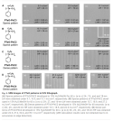
Polytelluoxane (PTeO) – based photoresists have recently attracted attention for extreme ultraviolet (EUV) lithography due to their high absorption efficiency and molecular-level homogeneity. In this work, we systematically investigate the plasma etch performance of a PTeO-based resist, with an emphasis on silicon pattern transfer and etch selectivity. Fluorine-based plasma chemistries were optimized by tuning inductively coupled plasma power, bias power, and gas composition. A CHF3/SF6 plasma with controlled additions of Ar and O2 was found to significantly enhance etch anisotropy and selectivity, achieving silicon etch rates exceeding 2µm/min and a maximum silicon-to-resist selectivity above five. Prolonged etching and post-lithography descum processes were further evaluated to assess profile stability and resist durability. In addition, effective pattern transfer into spin-on carbon layers was demonstrated. These results reveal the strong plasma robustness and substrate-dependent etch behavior of PTeO-based resists, highlighting their potential for advanced EUV lithography and pattern transfer applications.​

1784061735263.png1784061760883.png

Please, Log in or Register to view URLs content!
 
Top