Chinese semiconductor industry

Status
Not open for further replies.

ansy1968

Brigadier
Registered Member
That's what I thought.

Multi-patterning may require an additional precision or two on the machine but if what is being claimed that the machine is also capable (i.e. does have that additional precision) of doing multi-patterning for 14 nm is true, then the jump from 28 nm to 14 nm would be almost a given and relatively much easier and within a much shorter timeframe than the beginning work on building the 28nm process.
@Quickie bro the most difficult obstacle is jumping from 28nm Planar to 14nm FinFET. Since 7nm is also a FinFET going that route from 14nm is much easier as proven by TSMC by producing a 7nm DUVL chips as the machine is capable of doing using multiple patterning.

Now the next obstacle and challenge will be an EUVL, If China can able to deliver and successfully tackle the challenge, the implication will be huge as it broken the West hold on tech monopolies.
 
Last edited:

Xizor

Captain
Registered Member
You think civil engineering is ez pz?

if it's so easy then how come so many bridges and tunnels have collapsed the world over or cost untold fortunes?
No interest in doing the "ez pz" conversation here.

Semiconductor manufacturing involves different sciences and breakthroughs coming together. This is one area where "China speed" can be found lacking...and it's OK and understandable.

Semiconductors, Civil Aviation etc are extremely hard challenges that dare to defy "China Speed".
 

FairAndUnbiased

Brigadier
Registered Member
No interest in doing the "ez pz" conversation here.

Semiconductor manufacturing involves different sciences and breakthroughs coming together. This is one area where "China speed" can be found lacking...and it's OK and understandable.

Semiconductors, Civil Aviation etc are extremely hard challenges that dare to defy "China Speed".

Good thing China has a larger and more sophisticated semiconductor industry than even most developed countries then.
 

Quickie

Colonel
@Quickie bro the most difficult obstacle is jumping from 28nm Planar to 14nm FinFET. Since 7nm is also a FinFET going that route from 14nm is much easier as proven by TSMC by producing a 7nm DUVL chips as the machine is capable of doing using multiple patterning.

Now the next obstacle and challenge will be an EUVL, If China can able to deliver and successfully tackle the challenge, the implication will be huge as it broken the West hold on tech monopolies.

The experience of moving from 28nm Planar to 14nm FinFET has already been gained using the SMIC equipment. So the only thing to prove is the SMEE machine is the equivalent of the SMIC.
 

ansy1968

Brigadier
Registered Member
The experience of moving from 28nm Planar to 14nm FinFET has already been gained using the SMIC equipment. So the only thing to prove is the SMEE machine is the equivalent of the SMIC.
@Quickie bro to answer, can I borrow a phrase from our esteem member @superdog " how ever good the tools is , its still depend upon the skills of the Sculptor or a Painter to produce a masterpieces"
 
Last edited:

ansy1968

Brigadier
Registered Member
If Nikon can do it then in the future SMEE 28nm DUVL can, with the reports from my previous post of China Academy of Science had developed a 5nm laser lithography maybe they had plans and will work with SMEE to implement it in its future variants. I think SMEE or CETC may do a dual approach with its EUVL program and improving its DUVL. I'm speculating and forgive me for being an over enthusiast but a 5nm 3D DUVL chiplet will be competitive with the latest TSMC 3NM EUVL chip and if SMEE can improve the performance level comparable to NIKON and ASML NXT 2050i then it can buy some time for China IC especially Huawei, before the Chinese EUVL can be delivered in 2025.

From my friend @Oldschool

Nikon new immersion lithography can make 5nm, schedule to be on sale 2023.
Japan may not sell to CHina but this indicates DUV immersion can go beyond 7nm and down to 5nm.


Please, Log in or Register to view URLs content!


It can also process 5 nanometers! If you can't buy EUV, you can consider Nikon's new generation of ArF immersion lithography machine​

2021-10-24 13:06:36 Source: EETOP
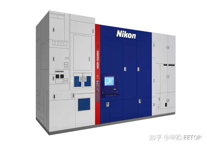
Nikon recently announced that it is currently developing the next-generation NSR-S636E ArF immersion lithography machine, which will provide excellent stacking accuracy and ultra-high throughput to support the manufacturing of the most critical
Please, Log in or Register to view URLs content!
equipment. Product sales are planned to start in 2023.

v2-d20468f18d545e7f61ce6218491ca632_720w.jpg


With the acceleration of digital transformation (DX), there is an urgent need to process and communicate large amounts of data very quickly. In order to meet these requirements, high-performance
Please, Log in or Register to view URLs content!
imperative, and
Please, Log in or Register to view URLs content!
device technology is constantly evolving. At the same time, attention is paid to the miniaturization of circuit patterns and the development of 3D device structures.
NSR-S636E-line alignment station having enhanced (iAS), which is integrated between the coater / developer unit and a lithography scanner
Please, Log in or Register to view URLs content!
pre-
Please, Log in or Register to view URLs content!
module. S636E and iAS utilize complex multi-point alignment
Please, Log in or Register to view URLs content!
and advanced correction functions to enable equipment manufacturers to achieve the strict overlay accuracy required for 3D equipment structures while maximizing the productivity of immersion lithography machines. NSR-S636E is very suitable for cutting-edge
Please, Log in or Register to view URLs content!
manufacturing, including logic and storage devices, CMOS image sensor applications, etc.
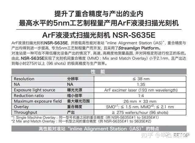
More about the NSR-S636E parameters have not been announced, but from the previous generation S635E claims may have been produced 5nm
Please, Log in or Register to view URLs content!
of view, S636E should at least be a more efficient way of producing 5 nanometer
Please, Log in or Register to view URLs content!
, and our country can not buy this for
Please, Log in or Register to view URLs content!
For the lithography machine, it is a good choice.

v2-f76f75280682d6ad0d29004fb6454573_720w.jpg

Please, Log in or Register to view URLs content!
 
Last edited:

ansy1968

Brigadier
Registered Member
I'm no expert and need some help, from the Spec given Nikon MMO is at 2.1nm while that of SMEE 28NM DUVL is at 2.5nm so the potential is there? need to boost its light source to able to achieved it? And also the wafer throughput is at 275/hour while that of SMEE is at 200, so the growth potential is there for SMEE 28nm DUVL and the gap is not that large?
 
Last edited:
Status
Not open for further replies.
Top