Chinese semiconductor industry

Status
Not open for further replies.

horse

Major
Registered Member
He is the SMEE Insider who gives regular updates on the progress of the DUVL.
He is always 100% reliable.
Recently however he hasnt been posting much.
There is a clampdown on such news recently.

That's means they are going to attack.

Business is not warfare, but both need strategy.

Trying to fake out your competitors, is standard stuff.

Then when you surprise them, you got'em on the run.

:D
 

Xizor

Captain
Registered Member
Nah, the West is about to die (literally), China will become the only market left.
No. This is a very naive and wrong perspective. The West is defined by its unique racio-cultural-ideological setup. It is as enduring as any other. The collective power of this entity called the "west" is still overwhelming.

A multipolar world is definitely possible. Not a unipolar China centric world.
I'm not sure why you'd be awaiting for 14nm mass production, given the domestic 28nm DUVL by all indicators has only recently had its initial units delivered, and a localized 14nm line is not expected until next year at the earliest.
Unless you're talking about a 14nm process in general (i.e.: non localized), in which case SMIC's 14nm line that produces SoCs such as Kirin 710A has existed since early 2020.

I thought I read here(likely) that 28nm had started production already at SMIC and 14nm was being worked on. If what you said is true then I'd readily peg China's progress even lower.

No, I'm not talking about non-localized fab line. But you are right that I often find the mix-up being a good cause for all the confusion.
 

ansy1968

Brigadier
Registered Member
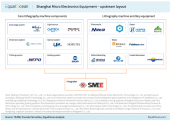
Not necessarily, there is quite a lot of movement in the Chinese semiconductor industry recently, but everything is kept under the radar to avoid attracting attention. Usually the progress is being published in low-profiles publications. SMEE launched a wide area lithography machine, which is quite significant because it is competing in the same area that Canon also wants to introduce itself, "Chiplets", to extend Moore's law. The announcement of this machine were published on their Chinese site but not in the English one. I think for the same reason of not attracting unwanted attention.
They probably have the machine already working but with this kind of machine is not like a commercial product that you produce yearly in mass like cars, this sophisticated machines have to pass a lot of validations by their primary costumers, in this case SMIC or others. Also this machines are going to be sold just to a few selected clients inside China with whom SMEE is collaborating, so even if they have the machine don't expect a big announcement until is certificated.
@tokenanalyst bro I'm intrigue if its okay for you to PM me the info or share it with us here. Thanks ;)
 

ZeEa5KPul

Colonel
Registered Member
I'm not sure why you'd be awaiting for 14nm mass production, given the domestic 28nm DUVL by all indicators has only recently had its initial units delivered, and a localized 14nm line is not expected until next year at the earliest.
The 28nm, 14nm, and 7nm processes use the same machines.
China is getting ready to ban TSMC from the 28nm and 14nm market. *wink*
TSMC is now an "unreliable entity" in those nodes.;)
 

tokenanalyst

Brigadier
Registered Member
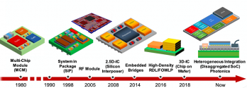
The growing demand for heterogeneous integration is driven by the 5G market that includes smartphones, data centers, servers, HPC, AI and IoT applications. Next-generation packaging technologies require tighter overlay to accommodate a larger package size with finer pitch chip interconnects on large format flexible panels.


Heterogeneous integration enables next-generation device performance gains by combining multiple silicon nodes and designs inside one package. The package size is expected to grow significantly, increasing to 75 x 75 mm and 150 x 150 mm, within the next few years. For these requirements, an extremely large exposure field with fine resolution lithography will enable packages well over 250 x 250 mm without the need for image stitching while exceeding aggressive overlay and critical uniformity requirements for these packages.


The lithography challenge to fulfill the need of heterogeneous integration is the limitation of exposure field size of the currently available solutions in the market. Multiple shots with stitching is used and this affects not only productivity performance but potential yield loss at the stitching boundary. Addressing the critical lithography challenges described above becomes an important task in heterogeneous integration, and an extremely large exposure field with fine resolution lithography is one of the best solutions for this task.

1635102801205.png
 

Quickie

Colonel
The 28nm, 14nm, and 7nm processes use the same machines.

TSMC is now an "unreliable entity" in those nodes.;)

The 28nm, 14nm, and 7nm processes use the same machines.

That's what I thought.

Multi-patterning may require an additional precision or two on the machine but if what is being claimed that the machine is also capable (i.e. does have that additional precision) of doing multi-patterning for 14 nm is true, then the jump from 28 nm to 14 nm would be almost a given and relatively much easier and within a much shorter timeframe than the beginning work on building the 28nm process.
 
Last edited:

krautmeister

Junior Member
Registered Member
@FairAndUnbiased @krautmeister @tokenanalyst bro had the EUVL reach the scale were it will be competitive against DUVL? with multiple FABS sprouting out in the US, EU and maybe Japan all using EUVL an infection point had been reach? Will it affect SMEE 28 DUVL and have a shortened career as China will obvious go with the trend and focus its attention?
Unless the capital costs of EUV drop dramatically relative to DUV, the coming EUV glut will simply cannibalize itself. EUV fixed costs already approach 50% of final product costs when fab capacity utilization is 80%+ and this high utilization requirement increases the closer to the leading edge we go. In other words, once global EUV capacity goes into overdrive, sometime after 2023, EUV capacity utilization will plunge and virtually every EUV fab will be losing money. If EUV fabs start competing on price, it will only magnify the problem. The chance that EUV can displace DUV market share is also "extremely" unlikely because of the inherent fixed cost and design cost advantages that >=7nm DUV process nodes have. When you factor in the coming of 3D chiplet proliferation, we're looking at an absolute catastrophe. It is more likely that DUV starts eating into the market share of EUV processes like 7, 5 and 3nm. This is like a baby deer in the headlights of an approaching freight train.

Thank you Ron Vara! If it wasn't for racist anti-China supremacists like this, China would continue following the globalist comparative advantage economic theory that keeps Anglo-American "allies" perpetual vassals.
 
Status
Not open for further replies.
Top