Chinese semiconductor thread II

tokenanalyst

Lieutenant General
Registered Member

Ultrathin aluminum layer-based DUV transparent thermal protection optical window​

Abstract​


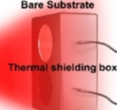
Extreme ultraviolet (EUV) light sources are critical for high-resolution lithography. For stable EUV output, real-time plasma monitoring is needed. However, broadband radiation of sources based on laser-produced plasma can induce thermal lensing in optical windows of detection systems, reducing observation accuracy and EUV generation efficiency. To solve this problem, thermal protection optical windows (TPO windows) are needed. Existing approaches, including multilayer all-dielectric coatings and transparent conductive coatings, often suffer from DUV absorption and fabrication complexity. This paper presents a DUV-transparent thermal protection window using an ultrathin aluminum (Al) layer. The fabricated TPO window achieved 67.7% transmittance at 266 nm, an average reflectance of 64% from UV to near-infrared (200–2500 nm) band, and over 96% in the mid-to-far infrared (2.5–11 μm) band. It also demonstrated excellent environmental stability, reducing thermal lensing by approximately 80% compared to bare substrates. These results indicate that ultrathin Al-based thermal protection windows are a practical and effective solution for enhancing the stability and measurement accuracy of EUV systems.
1762630574201.png

Please, Log in or Register to view URLs content!
 

jx191

New Member
Registered Member
<I. Technological Revolution in Domestic Lithography Machines

China's domestically produced lithography machines, employing laser-induced discharge plasma (LDP) technology, are expected to enter trial production in the third quarter of 2025. Featuring a compact design and a 40% reduction in energy consumption, this marks a significant step towards true self-reliance in the most cutting-edge semiconductor manufacturing field. This breakthrough may alter the traditional chip industry chain structure of "design abroad, manufacturing in East Asia, and application in China."

ASML, a traditional lithography machine giant, uses laser-induced plasma (LPP) technology in its EUV lithography machines. This technology relies on expensive and complex high-energy lasers to bombard tin droplets to generate plasma, and its control system is based on a precision FPGA. In contrast, the core of China's LDP technology lies in vaporizing the tin material between the electrodes and then converting it into a plasma state through high-voltage discharge. This "directional explosion" approach may be simpler and more efficient.

The Hyperion-1 prototype exhibits exciting features, such as a design that is one-third the size of ASML's, significantly reduced power consumption, and a clear manufacturing cost advantage. Although its power consumption is lower (50W vs. ASML's 250W), it has already achieved small-batch production of 5-3 nanometer nodes. Currently, its production capacity is approximately 10 wafers per hour, focusing on R&D and X-series chips. The plan is to launch Hyperion-2 by 2026, increasing production capacity to 150W/hour and achieving commercial production.>


Please, Log in or Register to view URLs content!
----------------
I know that post is controversial, but I think there are already EUV pilot lines in China, that is not just a EUV research lab, EUV pilot lines, a step closer to production, of course I think that the current systems are not even close to ASML, probably a few dozens wafers per hour like the post says, but the goal of 80 or even 100 wafers per hour by 2027 is a very high probability.
I think people inside this development in China already know where things are going and institutions and their companies are RUSHING to be first in the commercialization of EUV. I think, that most traditional supplier of lithography sub-systems like RS-Laser and Guowang Optical are now focus on KrF, ArF and ArFi, so they have to move fast.
Really interested stuff man. At this point it doesn't matter if China's EUV is only a couple dozen wafers per hour.

Even a dozen wafers would be enough to send the entire world into shock. Also the fact that we are seeing so many suppliers racing towards EUV shows that momentum is fast and they want to be at the front lines.
 

antiterror13

Brigadier
yep, GaN chip designers in China have quite the advantage.

Please, Log in or Register to view URLs content!

looks like SMIC is buying out the Beijing gov't controlled portion of SMIC North. This has 70k wpm of 12-inch capacity. Producing mostly 40 and 28nm chips.

It is kind of obvious by now that initial funding is more like loans in a way so that fabs can have the capital needed to build their fabs. Once they have the cash, they will buy back the remaining shares

I'd imagine the purchase value is significantly higher than original amount invested, so big profit for Beijing
 

tphuang

General
Staff member
Super Moderator
VIP Professional
Registered Member
I'd imagine the purchase value is significantly higher than original amount invested, so big profit for Beijing
well, investors typically need a return on their investment. If they put the money in 10 years ago, they'd want their investment to at least double by now.
 

sunnymaxi

Colonel
Registered Member
With a purity up to 8N, Jinggu Technology's ultra-high purity quartz materials are about to enter mass production.

Yangzhou Jinggu New Material Technology Co., Ltd. recently announced that it has successfully produced high-purity quartz sand of grade 7N and above through chemical reduction, and ultra-high- , as well as silicon-carbon composite materials, through synthesis. The company has achieved stable pilot-scale production and has completed the construction of its factory and production lines. Stable mass production will be gradually achieved soon!

Jinggu Technology claims that its high-purity synthetic quartz sand materials with a purity of 7N and above, and 8N, are oxygen-free and bubble-free, and are in the same category as products from Mitsubishi, Tosoh, and Shin-Etsu in Japan, and can replace similar products from Japan and the United States. This is not only the launch of a product, but also represents that the company has completely broken the international technological monopoly that has lasted for decades, and has a completely controllable independent product in the field of high-end quartz materials.

Please, Log in or Register to view URLs content!
 

tokenanalyst

Lieutenant General
Registered Member

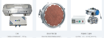
KBTES has secured tens of millions of yuan in Series A+ funding, and its products have passed verification by SMIC, CR Microelectronics, and other companies.​


Wuxi KBT Semiconductor Technology Co., Ltd. (KBTES) has successfully raised tens of millions of yuan in Series A+ funding, exclusively led by Tongchuang Venture Capital. The funds will support R&D innovation, capacity expansion, and market penetration, accelerating the localization of critical semiconductor components in China.

Founded in 2014, KBTES specializes in semiconductor vacuum components, particularly vacuum valves and heaters, areas long dominated by international players like Switzerland’s VAT. The company has broken key technological barriers, developing products that match global standards in precision, durability, corrosion resistance, and smart monitoring.
1762785135713.png
1762785169883.png
Its products have passed rigorous verification by major Chinese semiconductor firms—including SMIC, CR Microelectronics, Silan, BYD Semiconductor, and ACM Research Shanghai—and are now in mass production and delivery. Since 2024, KBTES valves have been deployed on 12-inch wafer production lines and in domestic equipment for cleaning and power devices, with a customer repurchase rate exceeding 85%.

KBTES employs a dual-track strategy, partnering simultaneously with equipment manufacturers and wafer fabs to drive localization at both system and facility levels. The company aims to grow the domestic market share of vacuum valves from 2% to 10%, and within three years, cover 90% of core valve models, while pioneering green, integrated solutions for sub-2nm advanced processes.

Please, Log in or Register to view URLs content!
 

tokenanalyst

Lieutenant General
Registered Member

Xi'an University of Technology establishes School of Integrated Circuits​

A conference on promoting the integration of industry and education and the convergence of science and education to support high-quality development was held, guided by the Shaanxi Provincial Department of Education, the Shaanxi Provincial Department of Science and Technology, and the Shaanxi Provincial Department of Industry and Information Technology, and hosted by Xi'an University of Technology.

To accurately align with national strategies and regional development needs, Xi'an University of Technology has established 13 new institutions, including the Undergraduate School, the Institute of Science and Technology, the School of Outstanding Engineers, the School of Future Technology (Zhixing Academy), the School of Artificial Intelligence Interdisciplinary Modern Industry (co-built with Huawei), the University Student Quality Education Center, the School of Mechanical Engineering, the School of Mathematics, the School of Ecology and Environment and Chemical Engineering, the School of Optoelectronic Science and Intelligent Instruments, the School of Integrated Circuits, and the School of Cyberspace Security. The guests at the meeting jointly unveiled the plaques for the new institutions.

The holding of this promotion meeting and the unveiling of the new institution are pragmatic measures taken by the university to implement the requirements of the "leading project" for building a strong education province. Going forward, the university will continue to deepen the integration of industry and education, and the fusion of science and education, demonstrating new responsibilities in serving the nation's high-level scientific and technological self-reliance and contributing to the development of new-quality productivity in Shaanxi, striving to write a new chapter of high-quality development.

Please, Log in or Register to view URLs content!
 

tokenanalyst

Lieutenant General
Registered Member

Xinju Semiconductor delivers glass substrate-related equipment to leading domestic customers.​


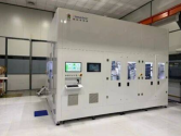
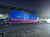
Xinju (Shenzhen) Semiconductor Technology Co., Ltd. (hereinafter referred to as "Xinju Semiconductor") successfully delivered its first fully independently developed electrochemical deposition (ECD) equipment to a leading domestic customer, achieving high-yield small-batch production to meet mass production requirements. This not only marks a significant breakthrough for my country in the field of key process equipment for high-end semiconductors, but also demonstrates the company's strength and confidence to compete with international advanced levels in the new race of "glass substrates," which determines the performance of next-generation chips, injecting strong momentum into ensuring the security and stability of the national industrial and supply chains.   
1762793629790.png1762793654171.png
It is reported that the ECD equipment and its supporting VCL etching equipment delivered this time were both independently developed by Xinju Semiconductor. Both the hardware and software were entirely self-developed, representing a completely new breakthrough in both technology and application. This equipment will be used in the core carrier of next-generation advanced packaging—the glass substrate. As Moore's Law approaches its physical limits, the path to improving chip performance is gradually shifting from "process miniaturization" to "packaging revolution." Glass substrates, with their ultra-low warpage, ultra-high surface flatness, and excellent high-frequency electrical characteristics, have become an ideal choice for 2.5D/3D integration and chiplet interconnection, achieving a 10-fold increase in interconnect density and a 30% reduction in power consumption, providing crucial support for high-end devices such as AI training and inference chips, high-bandwidth memory (HBM), and photonic integration. It is worth mentioning that the precision control of this ECD equipment in glass substrate manufacturing is currently the most difficult and critical manufacturing process in AI chip carrier processing.

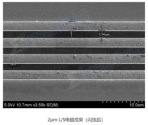
This equipment boasts high technical compatibility, supporting 12-inch circular glass chips as well as large-size square glass substrates such as 310×310mm, 515×510mm, and 610*610mm. It exhibits mass production stability with an RDL linewidth/spacing of 2 micrometers and a TGV deep via filling aspect ratio of 1:20. Its technical specifications have reached internationally advanced levels, with some key performance indicators even surpassing those of similar foreign products. This marks the first time that China's semiconductor industry chain has achieved the capability to compete on par with, and even surpass, international giants in certain areas of the "new glass substrate race."​

1762793820141.png

Please, Log in or Register to view URLs content!
 

tokenanalyst

Lieutenant General
Registered Member

S2C EDA showcased its digital EDA solutions at the 2025 China International Import Expo, empowering industrial innovation.​


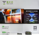
At the 2025 China International Import Expo, Sirchip's booth in the Lingang exhibition area received numerous visitors. As a representative company in the digital EDA field, Sirchip showcased a series of cutting-edge technologies and innovative achievements in chip design verification, attracting many professional visitors from home and abroad to stop and exchange ideas.

01 Highlights of the CIIE

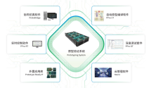
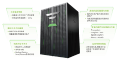
Silergy showcased tools for architecture design, software simulation, hardware simulation, prototype verification, and verification cloud services, demonstrating its comprehensive service capabilities for digital circuit design and implementation in fields such as artificial intelligence, high-performance computing, and image processing. Of particular note was Silergy's "ChipEye" prototype verification solution, embodying over two decades of technological accumulation. Its superior performance and continuous innovation made it an unsurprisingly popular exhibit in the area. A senior engineer from Japan stated at the event that Silergy's outstanding product capabilities and professional services are the fundamental reasons for their continued choice of the company.
1762795115761.png1762795137082.png

02 Addressing Global Chip Verification Challenges

With the rapid development of AI technology, the global integrated circuit design industry is facing unprecedented challenges. At the China International Import Expo (CIIE), a technology expert from Silergy pointed out: "The rapid development of AI applications has ushered in an era of hundreds of billions of gates in chip design, with software code volume surging to the hundreds of millions of lines, making design verification increasingly difficult." To address these challenges, Silergy has proposed three major development paths: a left-shift development strategy to provide overall solutions, in-depth cooperation with mainstream architecture and IP vendors to build an ecosystem, and the development of application-level innovative solutions adapted to emerging applications such as automotive and IoT.
1762795202628.png1762795268793.png

The company has already established strong partnerships with over 600 enterprises worldwide, and its products are widely used in terminal fields such as the Internet of Things, cloud computing, 5G communications, smart healthcare, and automotive electronics. Through the China International Import Expo (CIIE), Silergy has further expanded its international influence.

Please, Log in or Register to view URLs content!
 
Last edited:
Top