Contrary to popular believe Fujian Jinhua is not dead YET via XYZ
光刻机龙头ASML默默支持,福建晋华低调运转不停工
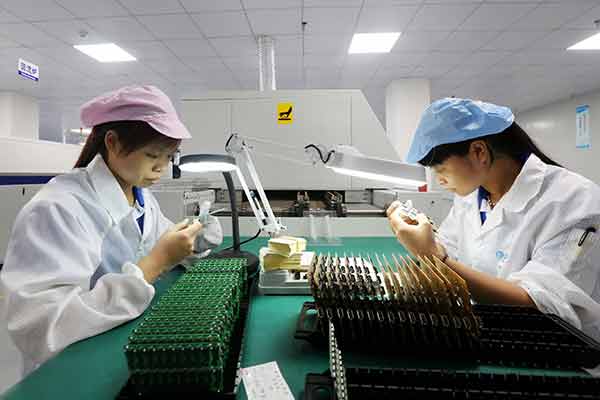
国内 DRAM 技术阵营福建晋华在被美方列入出口管制清单当日,所有美系设备商全数撤出,之后甚至传出整个工厂陷入停摆,然事实上,福建晋华仍是低调持续运转,且最大光刻机龙头 ASML 默默支持并未撤出,目前由福建晋华总经理陈正坤坐镇,采“龟息大法”维持工厂正常运作。
国内 DRAM 技术阵营福建晋华在被美方列入出口管制清单当日,所有美系设备商全数撤出,之后甚至传出整个工厂陷入停摆,然事实上,福建晋华仍是低调持续运转,且最大光刻机龙头 ASML 默默支持并未撤出,目前由福建晋华总经理陈正坤坐镇,采“龟息大法”维持工厂正常运作。
(来源:ASML)
2018 年 10 月 29 日美国一纸禁令宣布晋华被列为出口管制清单中,隔天 30 日,美系设备、材料等供应商全面撤出,包括机台安装、协助生产等动作也立刻停止,之后传出连非美系的供应商也撤出,整个 12 寸厂房呈现停摆状态。
事实上,目前福建晋华的 12 寸厂房仍是低调运转中,且光刻机大厂 ASML 并未如外传撤出,仍是默默支持,ASML 对 DT 君表示,会在符合各种法规要求的前提下,正常支持客户。
很显然地,虽然遭遇巨大冲击和压力,晋华也走到此一险境,但并没有放弃 DRAM 技术计划,现阶段的晋华员工仍是抱着没有退路的信念继续做下去,战到最后一刻。
受到晋华事件冲击,国内另一个 DRAM 技术阵营合肥长鑫的动态则是更为低调。
业界透露,合肥长鑫的 DRAM 芯片已经研发出来,良率也不错,但碍于眼前的“晋华风暴”,可能会延后量产。
再者,由于之前不少美光前员工加入合肥长鑫的团队,为了规避目前锋头正盛的 DRAM 专利侵权疑虑,长鑫也雇用不少来自前三星电子(Samsung Electronics)、 SK 海力士(SK Hynix)的韩国研发团队,竭尽所能地淡化美系色彩。
不过,传出之前“晋华案”爆发后,这些韩籍员工返回韩国后,有被当地政府“关切”,显示国内自制存储“芯”的风潮,仍是处于国际间的严密注视中。
眼前的福建晋华几乎是采用“龟息大法”在维持生命状态,让工厂的运作继续撑下去,但来自三面的压力仍是持续。一方面是来自美国司法部的起诉已在美国旧金山联邦法院开庭,晋华、联电提出无罪抗辩,争取从美国商务部出口管制清单中移除。
面对美国司法部的起诉,晋华和联电在美国分别寻找适合的律师协助处理该案,然而,晋华也遇到不少阻碍,主要是因为美国多家著名的律师事务所都与美系存储大厂美光(Micron)签约,而美光正是“晋华案”的幕后主要推手。
后来,晋华找到的律师为曾担任联邦检察官的 Christine Y. Wong,联电则是找来之前在美国欧巴马时代,担任联邦司法部助理总检察长的 Leslie R. Caldwell,作为辩护律师。
晋华遇到第二层面的压力,则是技术合作伙伴联电的终止 DRAM 技术开发计划。
根据原本规划,联电接受晋华委托的 DRAM 技术开发计画是在联电南科厂进行研发,待研发成功后,该组百人的 DRAM 研发团队将从联电转移至晋华,只是这组人还没转过去,美国的出口禁令就已经先一步出手拦截,现在这一组百人团队在联电已经内转到其他部门。
除了上述的美国司法大刀、合作伙伴退出 DRAM 技术开发计画外,晋华遇到的第三层阻碍是来自美系供应商的撤出。
2018 年 10 月底美国出口管制禁令一出,所有美系供应商包括 Applied Materials 、 KLA Corporation 、 Lam Research 、 Gatan 、 ECI Technology 、 Broker 、 Engegris 等全数撤出晋华,不过,部分非美系供应商并没有撤出,且晋华的晶圆厂仍是维持正常运作。
由于福建晋华先前已经采购可生产几千片的半导体机台设备,用以支应今年初进入小量投产,现在这些设备虽没有美系设备商人员协助生产,但晋华仍是想办法让机台正常运作,在耗材原物料方面,则是找韩系、日系的供应商代替美系的料源。
再者,合肥长鑫的 DRAM 技术开发计划是基于北京兆易创新、合肥市产业投资控股签署的《关于存储器研发项目之合作协议》,进行 19nm 工艺研发,总预算约为 180 亿元人民币,双方筹资比例为 1 :4,目标是在 2018 年 12 月 31 日前实现产品良率 (测试电性良好的晶片占整个晶圆的比例) 不低于 10% 目标。
兆易创新也于 2018 年 12 月 28 日公告,经沟通确认,双方约定合作的 DRAM 研发项目不会暂停
The lithography machine faucet ASML silently supports, Fujian Jinhua low-key operation does not stop
domestic DRAM technology camp Fujian Jinhua on the day of the US listed on the export control list, all US equipment vendors After the withdrawal, all the factories even went into a lockout. In fact, Fujian Jinhua is still in a low-key operation, and the largest lithography machine leader ASML silent support has not been withdrawn. Currently, Chen Zhengkun, general manager of Fujian Jinhua, is sitting. Adopting the "great method" to maintain the normal operation of the factory. On the day when the domestic DRAM technology camp Fujian Jinhua was listed on the export control list by the US, all the US equipment vendors were withdrawn, and even the entire factory was shut down. In fact, Fujian Jinhua is still low-key and continuous operation, and the largest The silent support of the lithography machine faucet ASML has not been withdrawn. At present, Chen Zhengkun, the general manager of Fujian Jinhua, is sitting in the town and adopts the “great interest law” to maintain the normal operation of the factory. (Source: ASML) On October 29, 2018, a US ban announced that Jinhua was listed as an export control list. On the next day, the US equipment, materials and other suppliers were fully withdrawn, including machine installation and assistance in production. The other actions were immediately stopped, and then the non-US suppliers were also withdrawn, and the entire 12-inch factory was shut down. In fact, the current 12-inch factory in Fujian Jinhua is still in low-key operation, and the lithography machine manufacturer ASML has not been withdrawn from the outside, and it is still silently supported. ASML said to DT Jun that it will meet various regulatory requirements. Under the premise, the customer is normally supported. Obviously, despite the tremendous impact and pressure, Jinhua has also come to this danger, but has not given up the DRAM technology plan. At this stage, Jinhua employees are still carrying on the belief that there is no retreat, and they will continue to do so. A moment. Affected by the Jinhua incident, the dynamic of another domestic DRAM technology camp, Hefei Changxin, is even more low-key. According to the industry, Hefei Changxin's DRAM chip has been developed, and the yield is also good. However, due to the “Jinhua Storm”, it may delay production. In addition, since many former Micron employees joined the team of Hefei Changxin, Changxin also hired many former Samsung Electronics and SK Hynix (SK) in order to avoid the current DRAM patent infringement concerns. Hynix's Korean R&D team is doing everything possible to downplay American colors. However, after the outbreak of the Jinhua case, these Korean employees returned to South Korea and were “concerned” by the local government, indicating that the domestic self-made storage “core” trend is still in the international close watch. In front of Fujian Jinhua, almost using the "great method" to maintain the state of life, let the operation of the factory continue, but the pressure from the three sides is still continuing. On the one hand, the lawsuit from the US Department of Justice has been held in the Federal Court of San Francisco, and Jinhua and UMC have pleaded not guilty and sought to remove it from the US Department of Commerce's export control list. In the face of the US Department of Justice's lawsuit, Jinhua and UMC searched for suitable lawyers in the United States to help deal with the case. However, Jinhua also encountered many obstacles, mainly because many famous law firms in the United States and the United States The storage giant Micron signed the contract, and Micron is the main promoter behind the Jinhua case. Later, Jinhua found the lawyer who was a federal prosecutor, Christine Y. Wong, and the company was Leslie R. Caldwell, who served as assistant attorney general of the Federal Ministry of Justice in the US Obama era, as a defense lawyer. Jinhua's second-level pressure is the termination of DRAM technology development plan by UMC. According to the original plan, UMC accepted the DRAM technology development plan commissioned by Jinhua to conduct research and development at UMC Nanke Factory. After the successful development, the group's DRAM R&D team will be transferred from UMC to Jinhua, but this group has not yet In the past, the US export ban has been intercepted first, and now this group of 100 people has been transferred to other departments in UMC. In addition to the above-mentioned US judicial slashers and partners withdrawing from the DRAM technology development program, the third obstacle encountered by Jinhua is the withdrawal from US suppliers. At the end of October 2018, the US export control ban came out. All US suppliers including Applied Materials, KLA Corporation, Lam Research, Gatan, ECI Technology, Broker, Engegris, etc. all withdrew from Jinhua, but some non-US suppliers There was no withdrawal and Jinhua’s fab was still operating normally. Since Fujian Jinhua has previously purchased thousands of semiconductor machine equipment, it will be used to support a small amount of production at the beginning of this year. Now, although these equipments are not assisted by American equipment manufacturers, Jinhua is still trying to make a machine. The station is in normal operation. In terms of raw materials for consumables, it is to find Korean and Japanese suppliers to replace the US source. In addition, Hefei Changxin's DRAM technology development plan is based on Beijing Zhaoyi Innovation and Hefei Industrial Investment Holdings' “Cooperation Agreement on Memory R&D Project”, which will carry out 19nm process research and development with a total budget of approximately RMB 18 billion. The fundraising ratio is 1:4, and the goal is to achieve a product yield (the proportion of wafers with good electrical conductivity to the entire wafer) of no less than 10% by December 31, 2018. Zhaoyi Innovation was also announced on December 28, 2018. After confirmation by communication, the DRAM R&D projects agreed by the two parties will not be suspended.