Indian Military News, Reports, Data, etc.

berserk

Junior Member
Registered Member
@ougoah both of these are GaN base AESA radar here from official brochure.

D107iiAX0AAxcN1 (1).jpeg

I posted this before but I think you didn't put to much attention which is expected. India may not have fabrication facility for commercial chip but for military purpose we already have state of the art one in GAETEC.

GAETEC is vertically integrated GaAs foundry comprising of design, wafer fabrication and Assembly,Testing and Reliability Evaluation facilities. GAETEC was established in 1996. This facility has been upgraded and now also have a GaN semiconductor fabrication facility.

another DRDO lab solid state physics laboratory (SSPL) is at forefront of development of many of these cutting edge technology specially GaN related semiconductor for strategic purposes. It hold many patents in this regard and is even ahead in many areas from its global peer's even from western nation. Here's a video.


Some screenshots
Screenshot_2020-05-01-02-33-44-75.jpg

Screenshot_2020-05-01-02-33-46-72.jpg

Screenshot_2020-05-01-02-33-51-22.jpg

Screenshot_2020-05-01-02-34-24-81.jpg

Screenshot_2020-05-01-02-34-25-79.jpg
 

ougoah

Brigadier
Registered Member
Appreciate the pictures. Do you have any GAETEC material in English, particularly in regards to projects/products they've already completed etc? To be honest, without captions describing what is happening in the pictures, we don't know what's going on. Especially considering there is a disconnect between GaN claims and out of context pictures. For example, GAETEC or DRDO explanations on what instruments and machinery are shown in the pics/vids and what they are being used to do.
 

ougoah

Brigadier
Registered Member
Great, look very outdated, what year was it? still with XP? ;)

Imagine how advanced the facility now (2020) ... woooow, just woww

To be fair, heaps of military branches and labs requiring certain securities use XP or obsolete Windows, including Chinese ones. These facilities are usually totally sealed off networks. US nuclear launch silos and control facilities often use absolutely antiquated equipment.
 

berserk

Junior Member
Registered Member
@ougoah I have already posted about it in this very thread couple of pages in reply to your own inquiry now you ask me again. Look like you don't read your own post's.

Please, Log in or Register to view URLs content!


You can read whole article here.

Please, Log in or Register to view URLs content!


From DRDO annual report.

IMG_20180602_101826 (2).png

images


IMG_20180602_101924 (2).png
 

berserk

Junior Member
Registered Member
Gallium Nitride (GaN)-based High Electron Mobility Transistor (HEMT) technology is revolutionizing the modern defence RF and electronic warfare systems. The capability of AlGaN/GaN HEMT to deliver high power, high frequency, high linearity, high efficiency and high temperature performance renders it the most sought after device for applications in advanced radars, data links, satcoms, etc. Particularly for RF power applications, GaN-based HEMT technology offers a significant advantage over the existing gallium arsenide (GaAs) Monolithic Microwave Integrated Circuits (MMICs). This is primarily due to the capability of GaN devices to operate at higher voltages owing to very high breakdown fields associated with them. Additionally, the GaN devices offer much higher impedance resulting in the requirement of less complex matching networks in RF power amplifier integrated circuits. On the whole, GaN technology results in minimizing the sizes of RF ICs by a factor of ten or even higher over the competing RF technologies. Moreover, the low current operation aided with a higher efficiency results in power saving and reduced costs for cooling the system. 
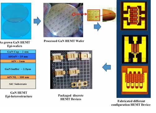
Therefore, the GaN-based power amplifiers constitute the heart of present day transceiver (T/R) modules in AESA (Active Electronically Scanned Array) radars and communication systems. To harness the potential of this technology, a project entitled AlGaN/GaN High Electron Mobility Transistors: Material and Device Technology Development (BALRAM) was undertaken by Solid State Physics Laboratory (SSPL) as a first step towards achieving long term self-reliance in GaN-based material, high power devices/MMICs for RF applications. SSPL evolved process control and characterization methodologies, besides, timely development of facilities for (a) epi-wafer growth and characterization, (b) device simulation, (c) device fabrication and (d) DC, RF and load pull measurement etc.

gan_orig.jpg


....................
 
Top