
You are using an out of date browser. It may not display this or other websites correctly.
You should upgrade or use an alternative browser.
You should upgrade or use an alternative browser.
Germany Carl Zeiss, heart of Dutch ASML Lithography Equipment.
- Thread starter tidalwave
- Start date
- Status
- Not open for further replies.
antiterror13
Brigadier
SMIC ordering more conventional lithography equipment from ASML for its 14nm production expansion. So, needless to say China pretty dependent on foreign tech on its IC production. The EUV project will enable China to shake up its status quo through industrialization of needed fundamental science tech.
Too many Chinese stuffs and research only live on papers.
Those are just general management jobs in the company, not even technical. Even if technical it's in process development , they can find better candidate from Taiwan and Korea. Those jobs wouldn't excite me.
My passion is in EUV lithography R&D.plucking up the hole, my last swan song in my technical career as I am already financial secured and ready to semi retire in couple more yrs.
EUV lithography or DUV lithography involved too many things, otherwise niche players like Taiwan or Korea would be all over them. The fact , they don't go into it shows how involved those projects are.
Last edited:
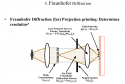
I am going to do small tutorial on optical system of lithography. It's beautiful tied together by mathmatical equation.
People are generally confused with the element of optical system such as the light source, condenser len(illuminator), the mask(design pattern), the pupil, and projection len and finally the wafer.
Light source ---gives out single frequency radiation
condenser (illuminator)--- transform the spherical light wave form (point source) into parallel rays to unifomlly shine on the mask
mask (design pattern)---- engineers design the circuit and design made into mask
Pupil ----- circular opening that allow the amount of light going into the projection len
Projection len------demagnification, or shrink 4x , 6x or 8x times smaller and have the the light coming through the pupil opening onto the wafer
Wafer---silicon Wafer
KEY IDEA: Diffracted light from any object is composed of many frequencies!
When single frequency of light shine onto the mask, the mask pattern will diffract the light into different frequencies therefore forms diffraction pattern, 0th, 1st, 2nd, -1st, -2nd.. 0th order contains more than 90% of the intensity. And normally one only need 0th and 1st. and the rest of them can be discarded.
Attachments
-
 1585119843107.png154.7 KB · Views: 17
The following picture beautifully tie everything together with set of mathmatical equation
1)The mask is represented by a mask transmittance function t(x1, y1)
When single frequency light shine go the the first len (condenser len), the mask diffracted the light into multiple frequencies and multiples order. This is equivalent of taking the mathmatical function Fourier Transform function on the mask function. And the result is Electric field E function E(fx, fy)
2)Then Pupil opening or Pupil function P(fx, fy) limit the entry of 0th, 1st and -1st order of diffracted light into the second len which is the projection len. The rest of the order 2nd, 3rd, -2nd, -3rd of the diffracted light got throw away.
3)The projection len perform an inverse Fourier Transform Function of the Electric field and pupil function.
or another word ,it gather back the diffracted (spread out) light , in this case 0st, 1st, -1st light and bring them all together and projected on to the wafer.
In summary, the optical system cause the single frequency light to diffracted or spread out by the mask, and then gather the needed light such as 0th, 1st, -1st and throw away the rest and projected the resultant light on the wafer. It uses Fourier transform and Inverse Fourier transform functions and tmask perform the Fourier transform and projection len perform inverse Fourier transform
EXCLUSIVE-U.S. OFFICIALS AGREE TO RULE-CHANGE TO RESTRICT HUAWEI FROM BUYING CHIPS MADE ABROAD WITH U.S. EQUIPMENT -SOURCES
China will answer this time, for sure.
Later this year, or early 2021 I will change my phone, so it's time to help Huawei.
#supportHuawei
Later this year, or early 2021 I will change my phone, so it's time to help Huawei.
#supportHuawei
Well, that was a matter of time. You could have predicted this months ago. I hope they have stockpiled enough for 2 years. That will give them some leeway to find solutions.
It all depends on whether Trump signs off on more sanctions against Huawei.
When this was almost agreed back in January, Trump blocked it.
So it would be very surprising if Trump signs off on more sanctions now, because Trump is shortly going to be asking Xi Jinping for medical supplies soon.
And I think for some chips, they change every 6-12months, so a 2 year stockpile wouldn't work in those cases.
It also looks like the Coronavirus will be a big issue in the USA for at least the next 3 months, so there is at least that long for Huawei to continue working on replacing US tech.
Last edited:
antiterror13
Brigadier
well, what "US Equipment" means? The only matter for Huawei is TSMC which produce its Kirin series at 7nm ... not sure whether US Equipment meant 5%, 10% or 25% (Currently the definition of "US equipment" is having 25% US components)
TSMC has said that its equipment to make 7nm have less than 10% US component
It will drive even faster to "De-Americanisation" of all software and hardware everywhere. America is no longer control all the technology in the world ... many countries could do that
TSMC has said that its equipment to make 7nm have less than 10% US component
It will drive even faster to "De-Americanisation" of all software and hardware everywhere. America is no longer control all the technology in the world ... many countries could do that
- Status
- Not open for further replies.